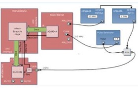
This reference design and the associated example Verilog code can be used as a starting point for interfacing Altera FPGAs to Texas Instruments' high-speed LVDS-interface analog-to-digital converters (ADC) and digital-to-analog converters (DAC). The firmware implementation is explained and the required timing constraints are discussed.
Features:
– This design is Firmware only and is discussed in detail to aid understanding
– Example Verilog code is an easy starting point for FPGA to high-speed data converter applications
– Design is easily expanded to other TI high-speed data converters
– The ADC and DAC portions are split in case only one is required
– Interface timing constraints are discussed in detail for the DAC and ADC
– Firmware was tested using readily available TI EVMs
Parts Included:
ADS4249: 14-Bit 250MSPS Dual Low Power ADC
DAC3482: 2-channel 16-bit 1.25GSPS Digital-to-Analog Converter
TPS74201: Single Output LDO, 1.5A, Adj.(0.8 to 3.3V), Any or No Cap, Programmable Soft Start
TPS74401: Single Output LDO, 3.0A, Adj.(0.8 to 3.3V), Fast Transient Response
TPS74701: Single Output LDO, 500mA, Adj. (0.8 to 3.6V), Programmable Soft-Start
TPS79618: Single Output LDO, 1.0A, Fixed(1.8V), Low Noise, High PSRR
TPS79633: Single Output LDO, 1.0A, Fixed(3.3V), Low Noise, High PSRR
Learn more by downloading the reference design below
Advertisement
Learn more about Texas Instruments


