Fundamentals of image sensors and processors
BY BRIAN DIPERT
Principal, Sierra Media
The image sensor is an increasingly prevalent semiconductor device found in digital still and video cameras, mobile phones and tablets, the bezels of laptop and all-in-one computers along with standalone displays, game console peripherals, and other systems. It attempts to mimic the photon-collecting and -processing capabilities of the human eye's retina:
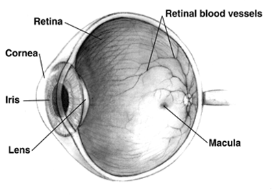
However, the retina's light-sensitive tissue combines two sets of photoreceptor cells; rods for grey-scale luminance measurement, and cones for color perception. Conversely, the image sensor is built of a uniform array of photodiodes and associated circuitry that's inherently sensitive to the entire visual light spectrum. Traditionally, sensor suppliers and their image processor partners addressed this functional gap by placing a multi-color filter array ahead of the sensor pixels. The most common filter combination, the so-called Bayer Pattern (named after its inventor, Eastman Kodak's Bryce E. Bayer), leverages the red, green and blue additive color pattern with twice as many green filters as either other color due to the human visual system's greater green-spectrum acuity:
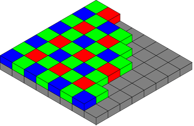
Post-capture image processing interpolates an approximation of each pixel's full-spectrum information, using partial-spectrum data captured both by each pixel and its surrounding neighbors. More recent advancements from Kodak and other companies add a proportion of all-white filters, trading off resolution accuracy for low-light performance, and some sensors instead harness a CMYK substractive-color filter pattern. The X3 image sensor, developed by Foveon (and now owned by Sigma), instead relies on the variable-depth absorption of various light frequencies within a semiconductor foundation, with successively located photodiodes capturing the red, green and blue spectrum specifics within each pixel's surface-area dimensions:
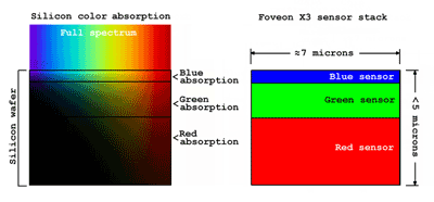
Up to the last few years, the CCD (charge-coupled device) was the prevalent image sensor approach. As the animated GIF that follows shows, electron charge packets accumulate in potential wells, and are sequentially read out of the device in a serial manner:
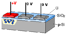
CCDs still find use in ultra-high-resolution applications, along with ultra-low-light environments such as astrophotography. However, they require custom semiconductor processing that not only has proven to be increasingly expensive versus the conventional bulk CMOS alternative but also limits the amount of beyond-sensor circuitry that can be integrated on the silicon sliver.
As such, the ascendant CMOS sensor quickly achieved widespread adoption once the resolution it could cost-effectively deliver became acceptable for volume applications. As Wikipedia concisely notes:
APS pixels solve the speed and scalability issues of the passive-pixel sensor. They generally consume less power than CCDs, have less image lag, and require less specialized manufacturing facilities. Unlike CCDs, APS [editor note: active-pixel] sensors can combine the image sensor function and image processing functions within the same integrated circuit; CMOS-type APS sensors are typically suited to applications in which packaging, power management, and on-chip processing are important.
CMOS sensors' pixel locations are capable of being randomly accessed and read out in parallel. The sensors commonly come in four-, three- and two-transistor per-pixel circuit configurations:
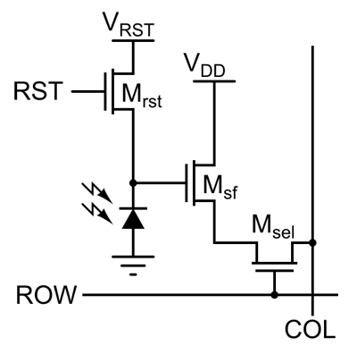
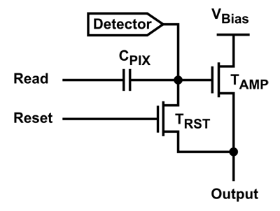
Large-pixel approaches often require anti-aliasing filters ahead of the sensor, which serve an analogous process to their audio processing counterparts; they slightly “blur” the image captured by the sensor in order to compensate for optics-enabled spectral response significant above the Nyquist frequency of 1/(2*pixel spacing). Aliasing often appears as a Moiré pattern on image regions containing high-frequency repetition, such as window screens and tight texture patterns. Alternative pixel structures such the earlier-mentioned Foveon sensor have less need for resolution-reducing anti-aliasing, as is the case with conventional sensors as their individual pixels decrease in size.
Moore's Law-driven pixel dimension shrinks enable cost-effective delivery of increasing image resolution over time, too, however they also degrade the sensor's low-light sensitivity by constricting each pixel's ability to collect sufficient photon data in a given amount of time. This undesirable tradeoff is particularly evident with low-fill-rate designs, in which the photodiode comprises a small percentage of each pixel's total surface area:
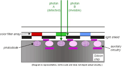
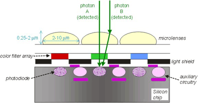
As partial compensation, manufacturers often place a micro lens arrays on top of the sensor:
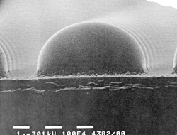
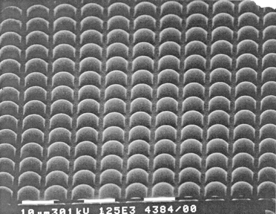
By “bending” the light as it strikes the sensor, each micro lens enables its correlated photodiode to capture more photon information:
Post-capture image processing is an equally critical factor in maintaining a camera's low-light capabilities as the all-important consumer eye-catching pixel count increases. Key to the processing algorithm's capabilities is differentiating between the desirable signal and the unwanted noise, and amplifying the former while ignoring (if not suppressing) the latter. Low-light enhancement is one aspect of the image processor's more general exposure responsibilities, aided in part by the various operating modes supported by modern cameras; “sports” which prioritizes high shutter speeds, “landscape” which prioritizes lengthy depth of field, “snow” which compensates for bright backgrounds, etc). But in the most commonly used “fully auto” mode, consumers still expect high-quality results, requiring (for example) that the image processor crank up the shutter speed when it detects high motion in the frame (aka small children, etc).
The image processor is also tasked with managing the LED flash illumination unit, as well as manipulating various lens functions; aperture, optical zoom, and focus. Traditional autofocus schemes, as with exposure, relied on spot-, center-weighted and full-scene-averaged algorithms. More recently, cameras can identify human faces within a scene and prioritize the focus point for those particular regions. And advanced cameras go beyond face detection to tackle more complex recognition tasks; waiting to trip the shutter until the subject smiles, for example.
The so-called “digital zoom” function attempts to elaborate on any existing optical zoom capabilities by cropping a portion of the sensor-captured scene and interpolating between “real” pixels to create the desired end resolution. Additional alteration modes viewed as desirable by some camera owners include conversion to old-time sepia tones, to black-and-white, and to a HDR (high-dynamic-range) version of the shot via auto-combination of a sequence of images rapidly taken at various exposure settings.
As image resolution in any particular dimension linearly increases, the processing “muscle” required to meet desired shutter-to-shot and shot-to-shot latencies exponentially goes up, although battery life impacts are generally unpalatable; fortunately, many algorithms are amenable to parallel-processing architectures. Once processing is completed, the image must be lossy-compressed and written to flash memory or another mass storage device. And of course, processing demands make a further notable uptick once a camera progresses from still-only image capture to standard- or high-definition video recording capabilities.
We're 30 years into the digital imaging revolution, if you measure its start by Sony's August 1981 unveiling of the Mavica electronic still camera, which recorded images to MiniDisc. Yet, the technology evolution and revolution pace continues unabated. One recent example is Lytro, who successfully demonstrated a prototype of its no-focus-required system in late June:

Lytro's approach harnesses the ever-burgeoning pixel counts of sensors, combined with the previously mentioned micro lens array, to capture both traditional light intensity and light ray direction. By varying the angles of micro lenses above close-proximity pixels, Lytro's scheme trades off effective sensor resolution for multiple stored copies of each pixel (therefore multiple image variants) at various focus points, which the camera owner can subsequently select among. ■
Advertisement
Learn more about Electronic Products Magazine


