Contributing Editor
Driven by increasing market demand for higher performance and more features, electronic systems incorporate larger numbers of sophisticated ICs, each presenting varying power requirements. At the systems level, the need to provide regulated power at multiple voltage and current levels presents a growing power management challenge. For engineers, the ability to leverage diverse power management ICs (PMIC) in systems design is fundamental for creating more power efficient designs, maximizing battery life in mobile applications, and providing proper systems functionality.
Power management circuitry ensures correct power flow in electronic systems. Besides maintaining power at the required voltage and current levels, power management circuitry is used to monitor power flows and provide alerts for supply faults such as under- and over-voltage levels that could damage sensitive application circuitry.
Power management circuitry is responsible for regulated power flows in ac/dc applications such as power supplies, computing servers, network infrastructure, industrial equipment, home appliances, and the like. At the heart of an ac/dc power supply, for example, power management circuitry senses voltage and current, adjusting power output as needed. Along with eliminating noise and transients introduced in the power line, more sophisticated power management subsystems also provide important capabilities including inrush current control, power factor correction for harmonic reduction compliance, and power metering for energy management applications.
Power management plays a vital role in dc/dc applications ranging from mission-critical automotive systems to battery-powered consumer electronics including notebooks, tablets, and mobile phones. For these applications, power management begins with voltage regulation through linear regulators or switching regulators.
Linear regulators offer a low-cost solution for providing a controlled output with a minimum of circuitry. In an archetypical linear regulator, a feedback loop maintains a constant voltage output despite changes in load (Fig. 1). In this feedback loop, a pass device responds to an error signal to adjust the voltage output to the desired regulated value. Because of the drop across the pass device, regulator operation requires a supply voltage that is greater than the output voltage. The minimum allowable difference between supply and regulated output is called the dropout voltage. For example, a 3.3-V regulator with 1-V dropout requires an input at least 4.3 V to operate.
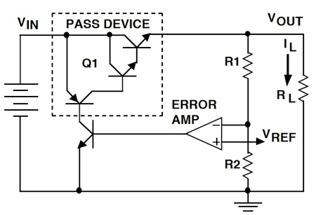
Fig. 1: In a standard linear regulator, a pass device responds to an error signal to maintain regulated voltage output. (Source: Texas Instruments.)
Low-dropout (LDO) regulators feature efficient pass device topologies that result in millivolt-level dropout voltages and provide a simple approach for providing a regulated output voltage from a higher voltage input. LDOs play a particularly key role in battery-powered applications due to their ability to use available power more fully and work deep into the battery discharge cycle. Semiconductor manufacturers offer LDO devices that provide additional power management features designed to aid in circuit protection. For example, LDOs are available with output pins for signaling faults due to thermal shutdown, low-power operation, and the like. Microcontrollers or other circuitry can monitor these fault signals and take appropriate corrective action.
Switching regulators have emerged as a favored option due to their higher efficiency and ability to use a single supply to provide voltages at different levels and polarity. Switching regulators are typically based on pulse-width modulation (PWM) of a square wave applied to an LC filter. Here, a feedback loop corrects the output voltage by changing the duty cycle of square-wave pulses delivered by a switch in the converter. The filtered square-wave pulses result in a dc output voltage equal to the duty cycle multiplied by the peak pulse amplitude.
Buck, or step-down, converters convert higher voltage supplies to lower voltages required by some circuits (Fig. 2a ). Boost, or step-up, converters provide the converse function, providing a voltage higher than the supply voltage (Fig. 2b ). Along with the basic buck and boost converter, converter manufacturers offer devices based on wide variations of these basic topologies to meet specific needs for voltage, current, efficiency, and functionality.
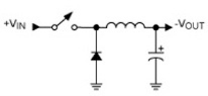
Fig. 2: Switched regulators can step-down, or buck, the supply voltage to a lower level (top) or step-up, or boost, the supply voltage to a higher level (bottom). (Source: Maxim Integrated Products.)
As systems grow in complexity, the need for more sophisticated power management has given rise to highly integrated PMICs that combine multiple LDO, buck, and boost converters on a single chip. These multi-converter PMICs are particularly vital for systems based on multiple custom ICs, ASICs, and FPGAs, which each present different power requirements. These parts typically include I2C-compatible serial interfaces that permit programmatic control of all regulators including output voltages and enable/disable control.
Beyond simplifying power design and reducing component count, however, advanced PMICs offer capabilities needed to implement more sophisticated power management techniques in system designs. For example, engineers can find PMICs that include real-time clocks, embedded controllers, and nonvolatile memory for supply monitoring, fault logging, supervision, and sequencing.
High-integration PMICs geared to specific application segments help engineers achieve further reductions in component count, system cost, and overall power consumption. For mobile applications, PMICs combine multiple converters with sophisticated battery charge and management features. PMICs for mobile phones offers features needed for RF power, including the ability to set output voltage of individual LDOs to different levels needed to optimize efficiency of RF power amplifier output. As a result, engineers can implement sophisticated power management for RF devices with a minimum of components (Figure 3).
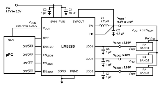
Fig. 3: Engineers can find PMICs optimized for specific applications such as power management of power amplifiers (PA) in RF designs, resulting in simpler designs and lower component count. (Source: Texas Instruments.)
While semiconductor manufacturers continue to deliver more efficient solutions, minimizing overall consumption requires power management methods at the system level. Engineers can use PMIC supervision and sequencing capabilities to power down unneeded circuits and use clock-gating schemes to reduce unnecessary clock transitions that contribute significantly to overall power consumption.
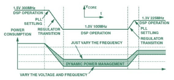
Fig. 4: Reducing both clock frequency and supply voltage can result in greater savings than possible with lowering frequency alone. In this example of dynamic power management, lower levels of both voltage and frequency achieve improved power savings in operation of a DSP device. (Source: Analog Devices)
Besides leveraging power-saving modes built into many components, engineers can apply techniques that modify system operating voltage or frequency to achieve significant power savings. In a CMOS logic gate, power varies linearly with frequency and with the square of supply voltage. Dynamic voltage scaling and adaptive voltage scaling techniques exploit this relationship between voltage and power by reducing voltage across the system to achieve power savings. Similarly, engineers typically reduce clock frequency in high-integration devices to lower system power consumption. With advanced PMICs, engineers can implement dynamic power management methods that take advantage of both methods to gain even greater savings (Fig. 4 ). ■
Advertisement
Learn more about Electronic Products Magazine


