GaN provides revolutionary improvements in power
GaN-based power devices will allow an order of magnitude improvement compared to systems based on silicon MOSFETs
BY MICHAEL A. BRIERE
International Rectifier
El Segundo, CA
http://www.irf.com
Within power conversion electronics, a general rule of thumb that has often been applied is that it is not possible to achieve high power density through high ratio conversion at frequencies above 10 MHz at the same time as achieving high conversion efficiency, without paying a large cost premium through complexity, such as in the use of resonant topologies. This is due to the generally slow, highly variable and lossy switching characteristics of the power devices used in the power conversion stage. From the advent of rectification, through linear regulation, the adoption of switch mode power supplies and resonant converters, power conversion topologies and the control circuitry that realize these architectures have been developed to take advantage of the inherent capabilities and avoid the deficiencies of the available power switch technology. When these power semiconductor technologies vary incrementally, it is advances in the architectures, drivers and control circuits which drive radical advances in power conversion electronics, such as multi-phase or sine wave conversion. However, on the rare occasion when the nature of the power switch itself changes radically, it is the nature of the power switch which drives radical, potentially revolutionary, changes in power electronics. Such a change is clearly approaching wide spread introduction in the near future. The general availability of commercially viable gallium nitride (GaN)-on-silicon based power devices provide the opportunity for more than an order of magnitude in performance improvement over state- of-the-art silicon devices within the next 5 to 10 years.
Currently, as the silicon based power FETs approach a performance plateau, cost of further enhancements are becoming prohibitively high. Concurrently, the next generation and emerging applications are demanding substantial improvements in power conversion performance.
Anticipating a need for a commercially viable new technology, scientists and engineers at IR have developed a revolutionary gallium nitride (GaN)-on-silicon based power device technology platform that promises to deliver cost effective performance that is at least ten times better than existing silicon devices, enabling dramatic reductions in energy consumption in applications like computing and communications, consumer appliances, lighting systems and automotive.
IR expects the potential impact of the new GaN based device technology platform, referred to as GaNpowIR, to be at least as significant as the introduction of HEXFETs some three decades ago.
GaN-on-Si-based power conversion
To fully exploit the benefits of these new GaN-on-Si based power devices, the GaN technology platform includes the development of complementary gate driver circuitry, advanced packaging solutions, as well as controller ICs and novel circuit topologies.
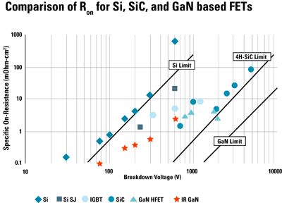
Currently, the basic GaN-on-Si structure is a high electron mobility transistor (HEMT). A combination of high conduction electron density, high electron mobility and higher bandgap provides GaN based HEMT devices with a significant reduction in device specific on-resistance RDS(on) for a given reverse hold off voltage capability compared with both SiC and silicon devices, as shown in the calculated material limit curves for (non-highly compensated) unipolar devices in Fig. 1 . Published measured results for FETs using the three materials, as well as highly compensated superjunction (SJ) and bipolar (IGBT) device structures in silicon are depicted for reference in this figure. In addition, results from the early stage development of the GaNpowIR technology platform (IR GaN) are also presented in Fig. 1. It is clear that an order of magnitude improvement in specific on-resistance can be achieved for GaN based devices over silicon counterparts, even at the early stages of GaN based power device development ( 30 years) or SiC ( > 20 years) technologies.

Fig. 1. Specific on-resistance of IR’s GaN-on-Si based high electron mobility transistors (HEMT)s compared to silicon and SiC powered FETs
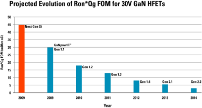
GaN based power devices achieve a combination of low gate capacitance and low on-resistance permitting much higher frequency efficient switching converters than do competing silicon transistors. Results based on device modeling, extrapolated from early measured results, indicate that R(on)*Qg FOM for first generation GaNpowIR HEMTs, to be introduced in 2009, is 33% lower than that of state of the art silicon MOSFETs. On going engineering efforts are expected to provide further significant improvements in the next few years. Figure 2 shows that R(on)*Qg for GaNpowIR devices is expected to be as low as 13 mΩ-nC by 2011. By 2014, the R(on)*Qg FOM for second generation GaNpowIR devices is expected to be less than 5 mΩ-nC, an order of magnitude improvement over state of the art Si based devices available in 2009.

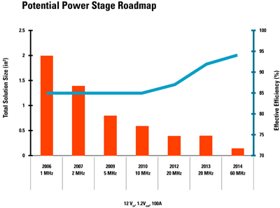
Fig. 2. Continuous improvements in GaN based HEMTs project an order of magnitude improvement in the R(on)*Qg figure of merit within five years of the introduction of GaNpowIR platform in 2009. Figure 3 illustrates the expected effect of the improvements in R(on)*Qsw FOM of the power switch on the size and efficiency of a dc/dc converter, including the output filter. Current state-of-the-art multi-phase silicon based solutions perform 12 V to 1.2 V conversion efficiently up to about 2 MHz per phase. The GaNpowIR technology platform is expected to enable efficient power conversion to greater than 50 MHz per phase in the near future. As can be seen, the improvements in the power switch FOM enable a corresponding increase in operating frequency with a substantial decrease in converter size, without a reduction in power conversion efficiency. The frequency shown in Fig. 3 is chosen to provide a constant conversion efficiency of 85%.

Fig. 3. Projected evolution of size and effective power conversion efficiency for a multiphase 100-A, 12 to 1.2-V dc/dc converter (including output filter). The per phase frequency shown on the timeline is chosen to provide a constant converter efficiency of 85%. The added efficiency above 20 MHz corresponds to reduced parasitic power loss downstream from the converter, made possible through the higher frequency conversion.
When the frequency is high enough (20 to 60 MHz), it eliminates the need for significant external components and the undesired distance between the converter and the load, achieving a significant reduction in parasitic related power loss. This provides an unprecedented combination of high density, higher efficiency and lower system cost. Consequently, using GaN based solutions, the dominant power conversion application FOM efficiency*density/cost will be considerably better than for silicon based alternatives.

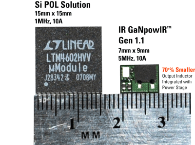
Fig. 4. GaN-on-Si based point-of-load (POL) converter switches at 5 MHz to deliver efficiency that is comparable to the state-of-the-art silicon solution running at 1 MHz, but at less than one third the size.
To demonstrate the distinct advantages of the new GaN-on-Si based power devices, several prototypes have been built. One such prototype is a low-voltage point-of-load (POL) converter. Designed for a 12 V input to 1.2 V output at 10 A load current, this GaN based (POL) converter runs at 5 MHz to deliver efficiency that is comparable to a commercially available silicon solution running at 1 MHz (Fig. 4 ), but at less than one third the size. Both solutions integrate the controller/ driver IC and output inductor within the power stage package. ■
Advertisement
Learn more about International Rectifier


