Getting it right for USB 3.0 circuit protection requirements
Paying attention to clamping performance and loading capacitance offers superior protection for high-speed USB 3.0 data lines
BY PETE PYTLIK, with contributions from JIM COLBY, CHAD MARAK, and COREY DEYALSINGH
Littelfuse
www.littelfuse.com
The market of USB-enabled devices is currently about three billion units a year. In 2010 the number of devices with USB 3.0 ports reached about 100 million units. This number will begin to increase rapidly in 2011 as more chipsets incorporate the new standard.
At data communication speeds of 5 Gbits/s, protecting these circuits from electrostatic discharge (ESD) just got more difficult. In addition to higher data rates, the USB 3.0 standard defines up to six data communication channels, and continuous shrinkage in IC geometries is making these circuits more susceptible to electrostatic discharge damage. The parasitic capacitance of a protection device has always been a major issue, but along with a low clamping voltage, these characteristics are now critical selection criteria for designers.
Some protection-device manufacturers have designed their products for a minimal parasitic capacitance to maximize signal integrity while others have maximized clamping performance at the cost of higher capacitance.
Understanding the tradeoffs between these selection criteria across the different protection technologies such as varistors, polymers, and silicon is key to achieving a successful design.
This article explains the issues in greater detail and shows USB3.0 eye diagram test results to prove why the right kind of silicon protection array is the best technology for protecting USB 3.0 applications against ESD.
USB 3.0 operating characteristics
Universal Serial Bus (USB) is a set of interface specifications for high-speed wired communication between electronic systems. Since the release of USB version 2.0 in 2001, data rates have increased from 480 Mbits/s to 5 Gbits/s in USB 3.0, as has maximum bus power and device current draw. The most significant change to USB 3.0 has been the introduction of two differential data pairs (see Fig. 1 ) called SSRx+/SSRx- and SSTx+/SSTx- in parallel with the existing data bus, thus increasing the number of connections from four to nine. This allows full-duplex simultaneous transfer of data as opposed to the single duplex unidirectional USB 2.0 bus. In addition to increased date transfer rates, the new specification also increases the amount of current available to power external devices. The maximum bus power output has increased from 500 to 900 mA.
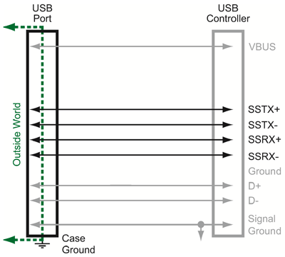
Fig. 1: USB 3.0 adds dual differential data pairs.
USB 3.0 circuit protection requirements
With the increase in data transfer rate to 5 Gbits/s and required decrease in channel capacitance in order support the new data rate, ESD protection used in previous generations of USB maybe inadequate for use with USB 3.0. Designers are more challenged with finding ESD protection solutions that can protect sensitive data lines without adding signal-distorting capacitance.
The introduction of additional differential data pairs requires more data lines to be protected against ESD then USB 2.0 and discrete ESD protection solutions used in the past to protect each individual data line may not be the ideal solution. New silicon array ESD protection devices, which are placed directly on the data pairs, not only protect legacy USB 2.0 data lines, but also these additional data signal pairs.
ESD threat overview
Interfaces such as USB 3.0 can be exposed to ESD by someone touching any of the pins on the connector or any of the pins on an open-ended cable connected to one of the ports. Even though modern IC chips often have some degree of protection (usually between 500 V to 2 kV), these ESD levels are based on the MIL-STD HBM model with 1,500-Ω resistance. With the MIL-STD model, 2 kV is closer to the IEC model at 500 V, which uses the 330-Ω resistor.
ESD events often can reach 15 kV or more and cause soft failures, latent damage, or catastrophic failure. Supplemental ESD protection is needed to enhance the survivability of today’s modern interface ports. To determine the immunity of systems to external ESD events, several test standards have been developed, with the International Eletrotechnical Commission (IEC) 61000-4-2 being most widely recognized. This standard defines ESD test levels that relate to different environmental and installation conditions and establishes test procedures. Today’s high-speed USB 3.0 ports must be able to survive a direct contact ESD of at least 8 kV, which is also an IEC 61000-4-2 level 4 requirement (see Fig. 2 ).
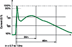
Fig. 2: IEC 61000-4-2 ESD current waveform.
Selecting the right protection for USB 3.0
Several different ESD suppression technologies such as MLV’s (Multi-layer varistors), polymer ESD suppressors and silicon are available on the market today and selecting the right protection will determine whether a USB 3.0 port will survive a discharge event or not. Some of the important parameters to carefully consider when selecting an ESD protection device are:
• Dynamic resistance.
• Off-state impedance.
• Multiple pulse stability.
• Parasitic capacitance.
• Package geometry.
Designers must be especially mindful of device capacitance, clamping voltage, and dynamic resistance as these parameters are critical in selecting the best ESD protection. Silicon-based devices such as SPA (silicon protection arrays) and diodes, with the lowest dynamic resistance, offer superior clamping performance and have one of the lowest parasitic package capacitances. Figure 3 illustrates clamping performance of silicon vs. MLV ESD protection technologies. As can be seen, Silicon-based solutions offer the lowest clamping voltage.
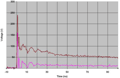
Fig. 3: Clamping performance of Si vs. varistor.
SPA TVS diode arrays
TVS diode array devices such as the Littelfuse SP3011 offer a multichannel ESD protection solution ideal for USB 3.0 protection. Littelfuse SPA devices work in two ways, first, they absorb the transient with diodes, to steer the current, and then, an avalanching or zener diode, clamps the voltage level. Figure 4 depicts a USB 3.0 ESD protection solution using a Littelfuse SP3011.
Offering six lines of ±8-kV ESD protection, and being able to protect both USB 3.0 differential pairs and legacy USB 2.0 data lines in a single package, Littelfuse SPA devices free designers from having to worry about using multiple ESD protection devices, which take up valuable board space.
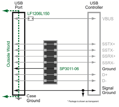
Fig. 4: USB 3.0 ESD protection using Littelfuse SP3011 device.
Signal integrity
Maintaining USB 3.0 data integrity is critical, and any small amount of added capacitance can cause signal distortion and degrade signal reliability. One way to evaluate what effect an ESD suppressor’s parasitic capacitance will have on signal integrity is to conduct eye-diagram testing. This test involves repetitively sampling a digital signal and displaying the resulting eye pattern on an oscilloscope. A mask is often used to define acceptable signal qualities and compliance.
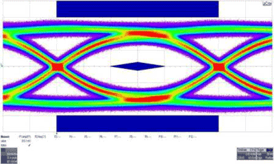
Fig. 5: Eye-diagram 5 Gbits/s.
Figure 5 displays an eye-diagram of a SP3011 silicon protection array using a 5Gb/s USB 3.0 compliance test pattern and mask. In order to simulate a real world USB 3.0 data path, test boards were designed with 90-Ω differential signal pairs and USB 3.0 connectors. It can be seen that signals are well within mask boundaries and wide eye width is maintained offering designers flexibility within a systems capacitance budget. ■
Advertisement
Learn more about Littelfuse


