A realistic option uses a concurrent flow
BY MICHAEL C. HEIMLICH
AWR, El Segundo, CA
http:// www.awrcorp.com
Smaller, faster, cheaper, . . . and more functionality. There are numerous ways to go about achieving these essential elements for today’s communication designs—none of them easy. Multi-technology design, while not a new concept, can provide a viable alternative for high-performance or high-function integration products if implemented with modern design tools and flows.
Multi-technology design is not without problems, of course. The biggest challenge is that it is “multi.” Multi-technology design spans all design domains: electrical/physical, circuit/system, design/analysis, etc., thereby making it challenging in its own right as a design methodology.
In order to design out the issues associated with multi-technology design, design flows comprising people, process, and electronic design automation (EDA) and computer-aided design (CAD) tools must be implemented. By portioning the design into a few, smaller functional blocks that map into smaller form factors and manufacturing each block in technologies that are selected with particular functionality in mind, the designer can implement “best-in-class” cost and performance criteria.
This article discusses how it is possible to leverage the benefits of multi-technology design and at what cost. With the availability of a useful, cost-effective design process, GHz multi-technology is a realistic option; without the design process, it is a product development nightmare and an unrealizable dream.
Problem definition
What do we mean by “GHz multi-technology design”? In the broadest sense, multi-technology design simply means that more than one manufacturing technology is being used to meet product requirements, including signals operating above 1 GHz.
The notion of multi-technology design has been used in its simplest form since the first integrated circuits where developed by placing a die in a package on a PCB. While the communications industry has made millions of successful products using multiple technologies, this has been done primarily with a highly compartmentalized, serial design flow.
The PCB design could ignore what was in the package to a large degree and the package design ignored what was on the IC. As frequencies and circuit densities have climbed, however, this compartmentalization is no longer possible.
Solution requirements
Multi-technology design really comes down to interconnects and interactions. Interconnects from one technology to another are critical from a design and manufacturing perspective because this is the weakest link now that each functional block has been optimized by technology selection. While each functional block may perform supremely in its own right, its integration with the rest of the system can be disastrous with improper interconnects.
Flow-based requirements
Traditional flows were very serial, as seen in Fig. 1 , mainly because there was plenty of design margin between system and component and between component and manufacturing. As frequencies and clock rates increased, secondary or parasitic effects crept in, and steps in the process were added to address these issues.
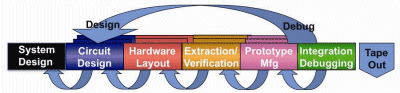
Fig. 1. As shown in a traditional design flow, three circuit components are designed in parallel and then integrated and debugged.
Today, these parasitics are anything but secondary as more and more challenging physics come into play at higher clock rates and densities. What is needed is a reordering of flow—essentially breaking the serial nature—to pull interconnect into circuit design through two complementary, not exclusive, approaches.
The first approach includes methodologies that encourage interconnect modeling in the design phase. This requires models and extraction tools. The second is the use of short, fast, moderately accurate EM tools during design. Fundamentally the biggest flow issue is that layout must be done inherently as part of circuit design, either by using parametric interconnect models or explicit layout.
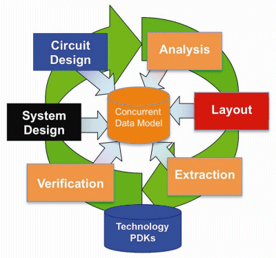
Fig. 2. In a concurrent design flow there are no barriers between technologies and design domains.
From a high-level perspective of design, these requirements imply a concurrent flow (see Fig. 2 ) from the electrical-physical perspective. In order to adequately design the interconnect, there must be a physical representation for it, however, in the traditional “waterfall” approach, layout is not begun until circuit design is completed. The notion of interconnect design is predicated on concurrency, and as a multi-GHz interconnect that is anything but parasitic, it cannot be accurately accounted for without first laying it out.
Point-tool-based requirements
While the reordering of the flow and its concurrency are key enablers for efficient and effective multi-technology strategies, the underlying point tools themselves are a key component. The issues here range from evolving capabilities to radical new technologies that heretofore may not have existed.
The ramifications of this feed directly into the circuit designer’s need for more accurate interconnect models and faster post-layout verification. Demands for the utmost speed, modest accuracy, and maintaining the highest degree of parametric control require the latest, most technologically advanced tools in both flows.
Cultural requirements
While the flow and point tool challenges can and are being addressed by the EDA industry, the cultural and structural issues within the actual product development group are perhaps the most daunting challenges in the electronics industry.
Since the concurrency necessary to accomplish efficient and effective multi-technology design requires a shift to the idea of layout as an electrical-based task rather than a physical-based task, there is tendency on the part of circuit designers to push back on learning a new discipline and CAD engineers to hold on too tightly to something old rather than embracing something new. The cultural leap is to accept the fact that the circuit designer is responsible for a “design complete” layout—one that ostensibly meets the electrical specifications with some minor homage paid to manufacturing issues—before the layout engineer picks it up and turns it into “production-ready” layout or the actual product.
As with any change, the real issue is, is it really needed? Incremental success and relatively minor additions and changes to processes, people’s skills and roles, and software tools have sparked a cultural confidence that since “the last design was successful,” the road the designer is on can be extended to the next project, and the next one, and the one after that. But what is not considered is that the last design was tougher and used up more of that precious margin or design resources.
The great “knock” against multi-technology design is that it makes the manufacturing more complicated. A greater emphasis is needed on ensuring that the design is manufacturable across the multiple component steps (such as individual die) and then across each integrating step (such as packaging or PCB).
Just as the shift from faster clocks to more cores has signaled a fundamental change in processor design, perhaps there are enough reasons to shift to a concurrent multi-technology flow with new tools and roles? ■
Advertisement
Learn more about Applied Wave Research


