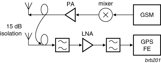
Description
Placing an external LNA close to the GPS antenna minimizes the NF, while the additional gain amplifies the GPS signal and raises the signal-to-jammer (on-board) ratio. In cellular phones with embedded GPS, this allows the GPS receiver to be close to the primary phone antenna for best GSM/UMTS performance, while having the GPS antenna as far away as possible for best antenna-to-antenna isolation, or for the best GPS antenna performance. Improved SNR also avoids non-compliance to 3GPP 25.171 and some UMTS channels.
Proven QUBiC4X process
Specifically designed for GPS receiver applications, the LNAs are produced in our industry-leading QUBiC4X process, a 0.25-µm SiGe:C technology. The proven QUBiC4Xi process improves overall RF performance and means the LNAs are less expensive and offer higher, more flexible performance than their GaAs counterparts. That means consumers always know where they are, and can receive continuous directions between high rise buildings or beneath heavy overcast skies. It also means having a GPS device that can run for days, instead of hours.
BGU7003 and BGU7005 LNAs
Optimized for small footprint and flexibility, the BGU7003 is ideal for GPS front-end modules. The BGU7005, optimized for a minimum of non-critical external components, is an excellent solution for discrete implementations of the GPS front-end. Both products have an enable function. In power-down mode, they consume less than 1 µA. They have very low noise figures and superior linearity performance, so they help improve overall sensitivity which in turn leads to faster TTFF and better tracking. The devices restore sensitivity, provide greater immunity against out-of-band cellular signals, reduce filtering requirements, and lower overall cost.
Download Full Block Diagram Below
Advertisement

Learn more about NXP Semiconductors


