The ball grid array (BGA) is a surface-mount chip package that is used to mount embedded devices (e.g. microprocessors) by melting balls of solder between the face of the device and the circuit board.
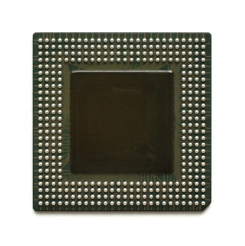
Unlike the perimeter-only package type, which place soldering pins along the edge of the device, a BGA aligns its solder balls in a grid beneath the bottom surface of the device. As a result, this approach leaves a considerably smaller footprint on the PCB and induces better thermal and electrical properties than a perimeter-style mounting package. It’s no surprise the format’s popularity has grown in tandem with the continuous miniaturization of electronics.
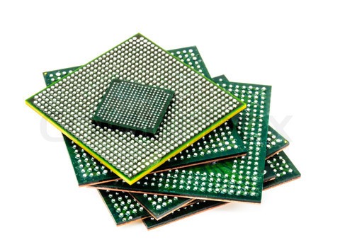
Bonding a device’s BGA with the copper trace pads on a PCB requires the use of either a reflow oven or infrared heating. These tools produce an even distribution of heat that melts each solder ball individually, effectively keeping the package aligned with pre-defined alignment indicators (pads) while the solder solidifies and forms the actual connection between the embedded device and the board.
The main disadvantage attributed with BGA usage is that soldering connections cannot be visually inspected once the device is mounted. The only way to test the BGA and eliminate the possibility of a soldering fault is through the use of X-ray machines, or such solutions. Poorly soldered BGAs can be removed and salvaged at a rework station, where they are replaced with new packets of solder balls, but repeated refurbishing will diminish the life expectancy of the embedded device to which they are attached.
A much better solution is to correctly place the BGA on the PCB from the beginning.
Placing BGAs and uBGAs
It is highly recommended that vias not be included in the track pads when using BGA in a PCB design. Vias and traces leading from the BGA that do not have a solder mask over bare copper are likely to cause solder thieving or poor solder joints, thus causing the BGA to fail. This is because solder balls arranged in a BGA will take any path they can when melting, often flowing away from its intended destination.
If the PCB design substitutes standard BGA packages with micro BGA (µBGA) packages, or ball grid arrays with a pitch of less than 0.5 mm, then paste flux may be used in place of solder paste. Keep in mind that uBGA’s smaller frame does not inhibit the board from being machine assembled; automated Pick-and-Placed machines handle uBGAs in much the same manner as other surface-mount components.
There is an exception to this rule: Certain pick-and-place machines are incompatible with µBGAs that feature a mirror surface due to vision issues. In these circumstances, the µBGA must be hand-placed. Contact the pcb assembly provider to determine if this may be an issue.
Testing
Finding a solder fault beneath a device whose packaged has been soldered into place is practically impossible without special equipment. Nevertheless, it is advantageous to do so in order to ensure optimal PCB performance.
Inspection tools include a range of devices: X-ray machines, industrial CT scanning machines, special microscopes, endoscopes, and JTAG. X-ray machines are arguably among the more efficient post BGA-bonding solutions due to their capacity for both 2D and 3D vision. The machines can see solder balls, excess solder, solder thieving, component misalignment, and bridging, as well as missing solder balls. This process helps verify that each solder ball is correctly placed, that each contact with the pads remains intact, and that no solder thieving has occurred.
The X-ray images below are examples of BGAs and µBGAs with various defects.
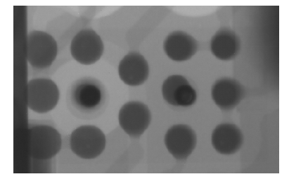
This 2D X-ray image depicts a µBGA suffering from solder thieving because its vias did not include a solder mask over bare copper. Notice how the solder balls have almost completely dissolved into the vias and created an open space.
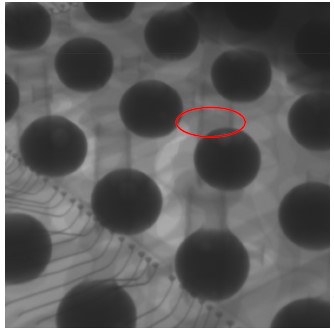
3D X-ray images of BGAs such as the one above permit an altogether different insight into the state of the BGA bonding. Here we see that the pad is visible at the top of each ball since the pad has a lower density compared to that of the ball.
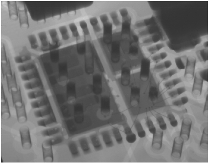
In this particular 3D image, we can easily see that a short has occurred under a plastic package.
Limitations
Unfortunately, there are some limitations when taking X-ray images. For example, it’s difficult to create a distinction between parts that are placed in the same location but on opposite sides of a board. Background metals such as POP parts may also create an interference with the X-ray that makes it image rendering difficult. As a result, exercising caution when aligning the BGA (or uBGA) with the PCB is ultimately the best practice; testing tools are simply meant to supplement accurate placement and provide a measure of quality assurance.
Advertisement
Learn more about Electronic Products Magazine


