Researchers at Georgia Tech have developed a polymer material that can reliably conduct heat from electronic devices. They accomplish this by harnessing an electropolymerization process to produce aligned arrays of polymer nanofibers. The team developed a thermal interface material that conducts heat 20 times better than the original polymer. This modified material can reliably operate at 200°C, a temperature that could make it useful for applications in vehicles.
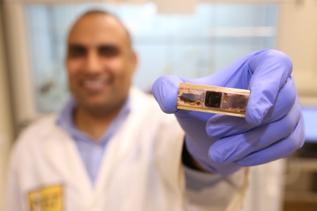
Research scientist Virendra Singh, from the George W. Woodruff School of Mechanical Engineering at Georgia Tech, holds a test sample used to measure thermal conductance and thermal cycle reliability in a new polymer material developed to remove heat from electronic devices. (Credit: Candler Hobbs)
The new thermal interface material could be used to draw heat away from electronic devices in servers, automobiles, high-brightness LEDs and certain mobile devices. The material is fabricated on heat sinks and heat spreaders and adheres well to devices, potentially avoiding the reliability challenges caused by differential expansion in other thermally conducting materials.
The research, which was supported by the National Science Foundation, involved researchers from the Georgia Institute of Technology, University of Texas at Austin, and Raytheon. Virendra Singh, a research scientist in the Woodruff School, and Thomas Bougher, a Ph.D. student in the Woodruff School, are the paper’s co-first authors.
The new interface material is produced from a conjugated polymer, polythiophene, in which aligned polymer chains in nanofibers facilitate the transfer of phonons — but without the brittleness associated with crystalline structures. Formation of the nanofibers produces an amorphous material with thermal conductivity of up to 4.4 W/m K at room temperature.
The structures are grown in a multistep process that begins with an alumina template containing tiny pores covered by an electrolyte containing monomer precursors. When an electrical potential is applied to the template, electrodes at the base of each pore attract the monomers and begin forming hollow nanofibers. The amount of current applied and the growth time control the length of the fibers and the thickness of their walls, while the pore size controls the diameter. Fiber diameters range from 18 to 300 nm, depending on the pore template. After formation of the monomer chains, the nanofibers are cross-linked with an electropolymerization process, and the template is removed. The resulting structure can be attached to electronic devices through the application of a liquid such as water or a solvent, which spreads the fibers and creates adhesion through capillary action and van der Waals forces.
The electrochemical polymerization processing approach enabled the researchers to align the chains of the polymer. The template appears to prevent the chains from folding into crystals so the material remained amorphous.
Though the technique still requires further development and is not fully understood theoretically, they think it could be scaled up for manufacturing and commercialization. The new material could allow reliable thermal interfaces as thin as 3 µm – compared to as much as 50 to 75 µm with conventional materials.
A patent application has been filed on the material, and a startup company, Carbice Nanotechnologies, to commercialize thermal interface technologies, has been formed.
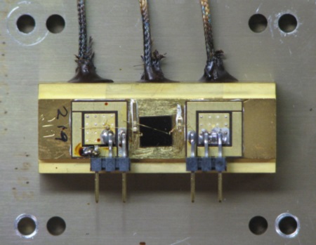
This image shows testing of a polythiophene nanofiber array grown on a copper heat sink and dried in contact with a silicon carbide RF device simulator. (Credit: Daniel P. Resler)
For more information – http://www.dx.doi.org/10.1038/nnano.2014.44
Advertisement


