Intel held an Architecture Day for the first time in two years; it was the company’s chance to reclaim the lead in technology innovation after some recent missteps. The company argued that future progress in IC performance will be predicated less on process shrinks and more on architectural innovations. It then went on to demonstrate it’s getting its groove back with work in several categories of architectural innovation.
Intel has codified those categories. Intel’s Raja Koduri, SVP, chief architect and GM Intel Architecture, Graphics and Software, focused on what Intel calls the Six Pillars of Innovation.

There are several variations of the six pillars of (or keys to) innovation. Raja Koduri explained Intel’s version. (Image: Intel)
They are: process (which included packaging), architecture, memory, interconnect, security, and software. Packaging is a critical element to putting heterogeneous design methodology together in an efficient coherent manner. And Intel had a lot to talk about when it comes to packaging. It is also clear that Intel has multiple arrows in its quiver to build future designs.
Raja called this the Architecture Era for the industry because just relying on process shrinks as the main driver of innovation is no longer the dominant way to improve system performance. It is going to take a lot of innovation on multiple fronts.
The event was a platform to communicate that Intel plans to be more flexible and adaptable in the future. With the issues Intel has had on recent 10nm and 7nm process shrinks, Intel is taking a “transistor resilient design” approach where designs can be targeted at Intel’s internal manufacturing capability or external foundries more easily. Intel is also migrating toward heterogeneous processing approach to compute scaling with scalar (CPU), vector (GPU), matrix (ML) and spatial (FPGA) architectures.
There was so much new information, I want to narrow it down to a few highlights.
Process and Packaging
While Intel did not address the latest production delay at its 7nm node, it did reveal a new technology for the existing 10nm node that will significantly improve transistor performance. The company made a number of innovations in silicon structures that in total deliver performance and power improvements almost equivalent to shrink to 7nm. Intel is calling this combination of features “SuperFin.”
The SuperFin technology includes an improved FinFET transistor with better drive current and improved channel mobility, and an improved metalization stack with a SuperMIM capacitor and lower resistance routing. The SuperFin allows for a wider dynamic range of processors with higher clock speeds and lower power. What is missing is the shrink of the transistor size to pack more transistors into the die area. This then puts more pressure on the design teams to get more performance out of the designs without growing die area.

(Click image for larger, clearer view. Image: Intel)
Previously Intel had differentiated transistor structure changes in existing process nodes by adding one or more plus (+) postscripts to the node name. Intel’s problem was that the pluses did not communicate significant transistor structure improvements. The hope is that a more descriptive name, like “SuperFin” will drive home that there’s a lot of transistor improvements taking place even if the node shrink isn’t there.
Intel is also turning to advanced packaging technology to build more flexible and more heterogeneous solutions. Intel is investing in 2.5D and 3D structures and other enabling technology like fine bump pitch and hybrid bonding. The company used its 2.5D EMIB technology for the Skylake-G module with discrete graphics in package and with its FPGAs. The most recent 3D Foveros technologies with Lakefield. Intel will also use packaging to more board level integration to package level integration — a critical technology for the company’s Client 2.0 architecture where chiplets are used to customize packaged processors for different market applications.
Intel will be releasing its AIB 2.0 die-to-die interconnect technology in early 2021 that will deliver up to 6.4Gbps per wire. With finer bump pitch it will significantly increase the bandwidth density for chip-to-chip communications. Intel also stressed AIB will be an open standard and will release the spec to the Chips Alliance Github.
The Foveros technology was first used by Intel’s first heterogeneous CPU design (Intel’s version of Arm’s big.little), Lake Field. Building on that design, Intel has another hybrid chip called Alder Lake which will focus on better performance than Lake Field; but will have Intel’s best performance/watt.
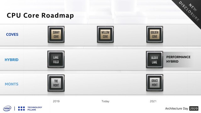
Intel’s CPU roadmap says the Alder Lake hybrid IC is scheduled for introduction in 2021. (Image: Intel)
Xe graphics and compute
A good example of how Intel’s process, packaging, and design work come together was the improvement in its new Xe graphics architecture used in the upcoming Tiger Lake processor. The GPU designers had to squeeze more performance out of basically the same amount of area. Part of those improvements were the result of SuperFin, but also a large amount of redesign was required to increase clock speeds and pack more compute units into the same die area as its predecessor. Intel was able to deliver a 2X performance improvement with the new GPU design.
Intel Xe GPU architecture product stack reaches from notebook processors all the way up to supercomputer math accelerators. Based on the scaling, it would seem to be a significant competitive threat to AMD and Nvidia. The development of Xe GPU is a critical part for Intel’s Aurora supercomputer design win with the “Ponte Vecchio” GPU accelerator.

(Click for larger, clearer image. Image: Intel)
As part of this more flexible approach to manufacturing Koduri revealed that the critical compute tile in Ponta Vecchio will be made by a foundry when it was originally planned to be manufactured internally. In the Ponte Vecchio design there are four different die that are packaged together — another example of Intel’s embrace of chiplet architecture.
The first members of the Xe family to ship will be the discrete graphics DG1 for mobile workstations and the Tiger Lake integrated GPU. Intel will also offer the SG1 for Servers streaming video and virtual desktops.

(Image: Intel)
Intel will be using packaging to scale the GPU architecture through a chiplet (“tile”) approach with multi-die packages for high performance compute applications. The HP version of Xe will focus on data center applications and programmability and with the scalability of using from one to four tiles in a module. The HP products should ship in 2021.
Another big reveal at Architecture Day was some details of the GPU for enthusiast consumer graphics. It will also utilize a chiplet approach to scaling when its released in 2021. The HPG version will also add hardware ray tracing support. We know it will be manufactured by an outside foundry (probably TSMC) and will use cost effective GDDR6 memory. It will also launch in 2021.
Tiger Lake CPU
The Tiger Lake integrated CPU shipping later this year will put the latest 10nm SuperFin process and the new Xe graphics architecture together for Intel’s best thin-and-light laptop processor. The “Willow Cove” CPU and Xe GPU in Tiger Lake benefit from a wider dynamic range of the SuperFin transistors for higher clock speeds, lower operating voltage, and lower power.

(Click image for larger, clearer view. Image: Intel)
Tiger Lake was also designed to compete better with AMD’s Radeon graphics with twice the performance of Intel’s previous mobile processor, Ice Lake. As such, Tiger Lake allocates more power to graphics and the more efficient Xe design has 96 execution units, up from 64 in Ice Lake and higher clock speeds. Tiger Lake should make an effective gaming processor and may also be able to support VR applications without a discrete GPU.
Another innovation in Tiger Lake is a gaussian and neural net (GNA) processor for ultralow power inference processing. The GNA 2.0 processor runs at 1GOP/mW. Very power efficient, but not high performance – sufficient for audio processing.

(Click image for larger, clearer view. Image: Intel)
Intel Looks to Gets Its Groove Back
There were also presentations on memory, networking, FPGAs, security, and software. Intel is moving ahead on many fronts. The tsunami of announcements at Architecture Day was designed to leave the audience with one impression – Intel has not stopped innovating and has a lot of new technology coming in the next two years.
To watch all of Intel’s Architecture Day presentation, they are all online at this web page.
The article originally published at EE Times.
Advertisement
Learn more about IntelIntel Corp.


