By Steve Knoth, senior product marketing manager, Analog Devices’ Power Group.
Sophisticated high-power-density digital integrated circuits (ICs), such as graphics processor units (GPUs) and field programmable gate arrays (FPGAs), can be found in a broad range of feature-rich electronic environments, including automotive, medical, telecom, datacom, industrial, communications, gaming, and consumer audio/video. High-power-density digital ICs have penetrated virtually every embedded system.
With this level of market penetration, it is no surprise that the global demand for high current, low voltage digital ICs is exploding. The current global market is assessed at more than $1.8 billion, and this is expected to rise annually by 10.87% to reach $3.7 billion over the 2018 to 2025 period.
As one of the biggest slices of this market, FPGAs account for a projected $1.53 billion by the end of 2025. The rest of the digital IC market is represented by GPUs, microcontrollers and microprocessors, programmable logic devices (PLDs), digital signal processors (DSPs), and application-specific integrated circuits (ASICs).
FPGAs enable cutting-edge applications in the market segments listed above. For example, in automotive applications, advanced driver assistance systems (ADAS) and collision avoidance systems prevent catastrophe due to human error. Likewise, government-mandated safety features such as anti-lock brake systems, stability control, and electronically-controlled independent suspension systems require FPGAs to function.
These digital ICs are powerful, yet temperamental, especially regarding power requirements. Traditionally, efficient switching regulator controllers that drive high power MOSFETs have been used to power FPGAs and ASICs, but these controller-based power schemes have potential noise interference issues, relatively slow transient response, and layout limitations.
Switching regulators vs. charge pumps vs. LDO regulators
Low voltage, high current step-down conversion and regulation can be achieved via a variety of methods, each with its own performance and design trade-offs. Switching regulator controllers feature high efficiency at high load currents over a wide range of voltages, but they require several external components such as inductors, capacitors, and FETs to operate, and they can be a source of high and low frequency noise. Inductorless charge pumps (or switched capacitor voltage converters) can also be used to produce low voltages, but are limited in output current capability, suffer from poor transient performance, and require several external components. For these reasons, charge pumps are not commonly found in digital IC power applications.
Linear regulators — especially LDO regulators — are simple in that they only require two external capacitors to operate. However, they may be power limited depending on the size of the input-to-output voltage differential across the IC, and how much current is demanded by the load, plus the thermal resistance characteristics of the package. This certainly limits their ability to power digital ICs.
Monolithic buck converter design challenges
Moore’s Law has proven to be visionary and valid since its debut in 1965. Wafer fabrication technology line widths are continually being reduced, pushing digital IC voltages lower. Smaller geometry processes allow higher integration of more power-hungry features in the end product.
For example, modern computer servers and optical communication routing systems demand higher bandwidth to process more computing data and internet traffic; these systems also generate a lot of heat, and therefore highly efficient ICs are required. Cars have more on-board electronics for entertainment, navigation, self-driving features, and even engine control. As a result, there is an increase in both the system’s current consumption and the associated total power required. Therefore, state-of-the-art packaging and innovative, internal power-stage design are required to drive the heat out of the power IC while delivering unprecedented power.
High power supply rejection ratio (PSRR) and low-output voltage noise, or ripple, are important considerations. A device with high supply rejection can filter and reject noise at the input, resulting in a clean and stable output. Furthermore, power solutions with low-output voltage noise across a wide bandwidth or low-output ripple are desirable — modern digital systems have several rails where noise sensitivity is a major design consideration.
As speed requirements for high end FPGAs increase, supply noise tolerance decreases in order to minimize bit errors. Noise-induced digital faults drastically reduce the effective data throughput speeds for these high speed PLDs. Input supply noise at high current is one of the more demanding specifications placed on power supplies.
Higher transceiver speeds, in FPGAs, for example, dictate high current levels due to high power consumption from fine geometry circuit switching. These ICs are fast. They may cycle load current from near-zero to several amps within tens to hundreds of nanoseconds, requiring a regulator with an ultra-fast transient response.
With board area reserved for the power regulators ever-decreasing, many system designers turn to monolithic switching regulators operating at fast switching frequencies to reduce the size of external components and total solution size — accepting the trade-off of some efficiency loss due to switching losses at higher frequencies.
This trade-off is eliminated by a new generation of monolithic switching regulators. These new regulators feature synchronous operation with integrated high-side and low-side switches, allowing for tight control of switch gate voltages, greatly reducing dead time, and resulting in higher efficiencies even at high frequencies.
It’s clear that buck converter solutions for high performance digital ICs must have the following attributes:
- Fast switching frequency to minimize the size of external components
- Zero dead-time design to maximize efficiency at high frequency
- Monolithic chip on-board power device for smaller solution size
- Multi-phase operation to enable parallel operation for high output currents and reduced ripple
- Low EMI to meet low system noise requirements
- Synchronous operation for high efficiency and minimal power loss
- Easy design to simplify design cycle, qualification, and testing
- Very low output ripple
- Fast transient response time
- Operation over a wide input/output voltage range
- High output current capability
- Excellent thermal performance
- Compact footprint
Traditionally, digital ICs has been powered by LDO regulators or inductor-based switching regulator controllers with off-board power devices. With increased power supply performance and space requirements, in many cases these traditional approaches cannot meet these requirements.
ADI’s new generation of monolithic power supplies, as an example, including the LTC3310S, LTC3309A, LTC3308A, and LTC3307A, which support 10 A, 6 A, 4 A, and 3 A, respectively, are up to the task. These high-power-density Silent Switcher and Silent Switcher 2 buck regulators are housed in thermally efficient, compact flip-chip laminate packages, and offer a variety of feature sets to satisfy the requirements of a wide range of digital IC power problems.
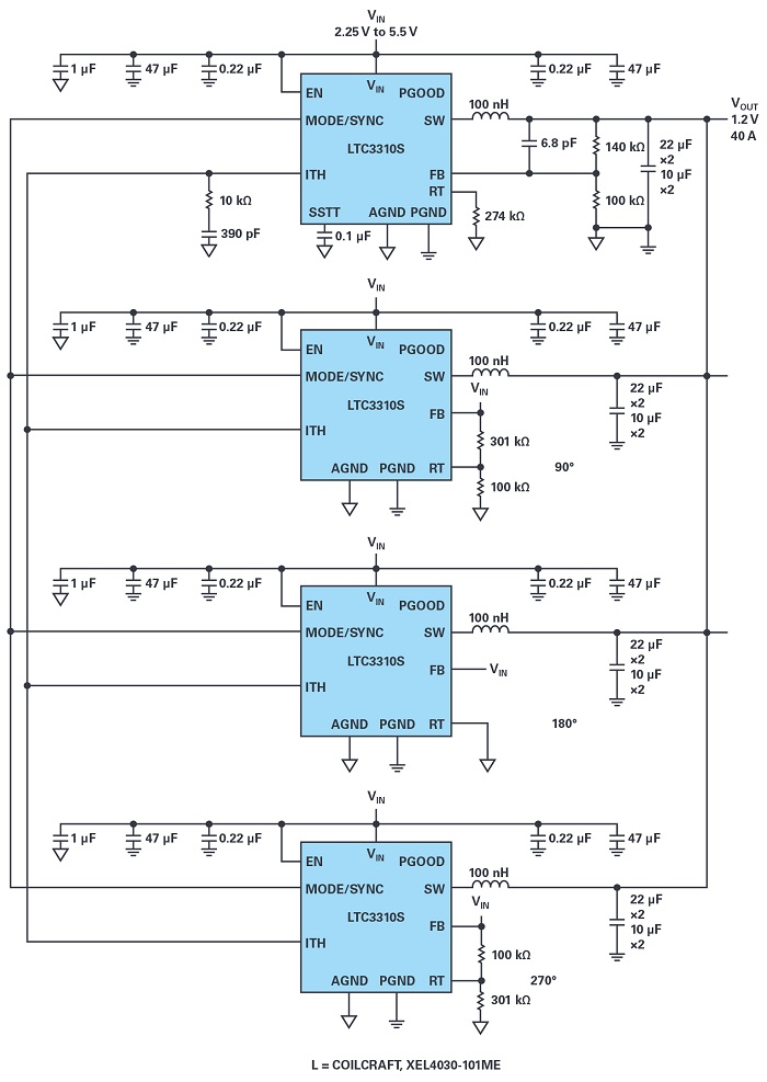
Fig. 1 Four LTC3310S monolithic regulators in parallel, forming a four-phase, 40 A step-down regulator.
Table 1 compares the features of the LTC33xx Silent Switcher and Silent Switcher 2 family.
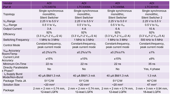
Table 1: Fault mode and supported range.
Conclusion
The trend in high performance digital ICs — such as GPUs, FPGAs, and microprocessors — is rapidly raising current demands coupled with dropping operating voltages, a result of shrinking line width wafer fabrication technologies. Current and voltage demands are only part of the power supply picture. Digital IC advancements come with a host of other requirements, including fast transient response, low EMI, low noise/ripple, and efficient operation to minimize heat.
About the Author
Steve Knoth is a senior product marketing manager in Analog Devices’ Power Group. He is responsible for all power management integrated circuit (PMIC) products, low dropout (LDO) regulators, battery chargers, charge pumps, charge pump-based LED drivers, supercapacitor chargers, and low voltage monolithic switching regulators. Prior to rejoining Analog Devices in 2004, Steve held various marketing and product engineering positions since 1990 at Micro Power Systems, Analog Devices, and Micrel Semiconductor. He earned his bachelor’s degree in electrical engineering in 1988 and a master’s degree in physics in 1995, both from San Jose State University. Steve also received an M.B.A. in technology management from the University of Phoenix in 2000. In addition to enjoying time with his kids, Steve is an avid music lover and can be found tinkering with pinball and arcade games or muscle cars, and buying, selling, and collecting vintage toys, movie, sports, and automotive memorabilia. He can be reached at steve.knoth@analog.com .
Advertisement
Learn more about Electronic Products Magazine


