By CARL BLAKE, Senior Advisor, Marketing,
Transphorm,
www.transphormusa.com
At every step in the adoption GaN (Gallium Nitride) products, there has been widespread skepticism among engineers about the reality using this technology. Many still find it surprising that GaN replaced SiC in the LED market in 18 months and in the RF amplifier market in three years. Although the transition to GaN in the power device market isn’t expected to occur as rapidly, a growing number of companies are finding that using GaN is not only possible, it can result in higher-performance and smaller, more efficient designs.
600 V, JDEC-qualified, normally off cascade HEMTs (high electron mobility transistors), which are compatible with existing drivers and controllers, are making it easy to use GaN in power applications, with minimal changes beyond improving layouts and optimizing designs for higher frequencies. Engineers are beginning to design GaN circuits into their applications to take advantage of the low output capacitance, extremely low reverse recovery, and the high-voltage spike tolerance demonstrated by rugged HEMT devices. This article describes GaN solutions that companies have already adopted for their power applications.
GaN PV inverter
The first commercial adoption of high-voltage GaN was in a PV inverter introduced by Yaskawa. This Japanese company has a history of advancing new technology, such as being the first to convert from bipolar transistor-based inverters to IGBT-based inverters in the motor drive control industry. Their adoption of GaN began with a simple inverter demo board (see Fig. 1 ) that demonstrated the new tighter layouts that would be required when replacing IGBT based solutions with GaN-based solutions. The key to this insight was not just the switching frequency of 50 kHz (compared to 15kHz in previous designs using IGBTs), but the very high dv/dt and the ultimate low reverse charge of the GaN HEMT, which led to achieving extremely low switching losses. Once designers understood the layout demands, the balance of the system design became an exercise in how best to extract the full benefits of the 600 V GaN HEMTs. This was achieved by integrating a synchronous boost circuit with a high-efficiency bridge inverter that enabled a 40% size reduction plus a 40% reduction of the losses.
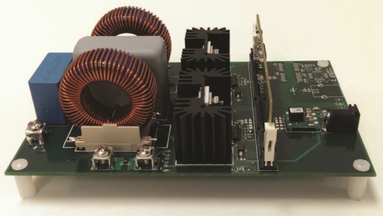
Fig. 1: Single-phase 1 kW Inverter demo board.
Transphorm’s evaluation kit (TDPV1000E0C1) provides designers with an easy way to evaluate the performance advantages of GaN power transistors in single-phase inverter applications, such as PV or UPSs (uninterruptible power supplies). In this kit, four GaN HEMTs are configured as a full bridge, switching at 100 kHz or higher to generate a sinusoidal AC output amplitude of 100 V up to 240 V from a 400 Volt DC bus. The output power of 1000 W is achieved without forced air cooling, although with forced air cooling more than 1500 W is possible.
Bridgeless totem pole
The demand for higher-efficiency power supplies for datacom and telecom systems spurred the interest in bridgeless topologies to eliminate the fixed diode drop, which at 115 Vac line equals 2%, making the achievement of 98% overall efficiency impossible. Although, highly efficient, many designs based on this type of topology can have significant EMI (electromagnetic) issues with conducted emissions. Another potential drawback of this topology is that its high component count consumes a large amount of PCB (printed circuit board) real estate. However, one bridgeless topology, the totem pole, offers the benefits of high efficiency along with improved EMI and low component count. This means that for the first time it is possible to reach 98% ac line to dc output at the 50% load point. (This is key to meeting the long-term roadmap published by IBM and other large computing manufacturers, as well as for meeting LEED building standards for energy efficiency.)
Transphorm’s demonstration board (TDPS500E2A2) for its totem pole bridgeless topology implementation consists of two GaN HEMT and two silicon MOSFETs (see Fig. 2 ).
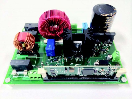
Fig. 2: Totem-pole PFC demo board.
As illustrated in Fig. 3 , the operation principle of the totem pole PFC topology is best explained by breaking the bridgeless PFC into two half-cycle circuits. These consist of: S1 and SD1 as one half-cycle bridgeless PFC and S2 and SD2 as a second half-cycle. In the positive AC line half-cycle, SD2 conducts and connects the AC source to the output ground. S2 is the active boost switch. In the negative AC line half cycle, SD1 conducts and connects the AC source to the output DC bus. S1 is the active boost switch. The operation mode changes at each AC zero-crossing. In the positive half, the PWM that is determined by boost duty ratio is driving switch S2, while it is driving switch S1 in the negative half.
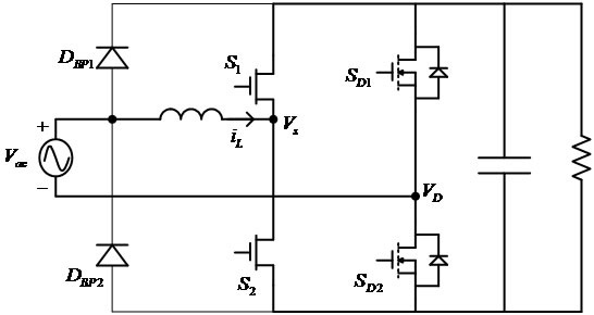
Fig. 3: Synchronous totem pole circuit for bridgeless PFC.
Based on the above operation, switch S1 and S2 work as freewheeling diodes in the boost circuit. The large reverse recovery charge (Qrr) of the existing silicon MOSFETs would make the CCM (continuous conduction mode) operation of the totem pole bridgeless PFC impractical. Compared to using a typical super junction transistor, a GaN HEMT’s low Qrr and low switching loss make it the perfect power device for this topology.
All-in-one
The most recent demo board (TDPS250E2D2), as shown in Fig. 4 , from Transphorm is a reference design for a 250- W power supply targeted for all-in-one computers and other low-power applications where size and efficiency are desired. This design was born from collaboration between ON Semiconductor and Transphorm that demonstrated GaN solutions offer value in consumer applications down to a couple hundred watts. The demo boards were first shown at APEC 2014 and the reference design was released in September 2014.
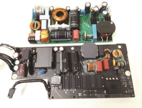
Fig. 4: A 250 W all-in-one power supply reference board.
Additionally, Transphorm has designed a complete evaluation board for a 250 W power supply specifically to meet the requirements for an all-in-one computer. The evaluation board uses ON Semiconductor control ICs (NCP4810, NCP1654, NCP1397, NCP4304, and NCP432) and three Transphorm 600 V GaN HEMTs in both the PFC and resonant bridge circuits to achieve the higher performance that enables smaller flatter systems.
This application takes advantage of the improved performance of GaN HEMT transistors, not only in the hard-switched PFC circuit but also in the resonant bridge circuit where the very low output capacitance of the GaN HEMT transistor enables faster discharge of the stored energy, and thus reduces the losses. The compact-size board is designed to switch at 200 kHz in order to shrink the size by 45%. It also simultaneously reduces the losses by 30% to achieve the target efficiency of greater than 95%. This showcases the advantage of using GaN devices for achieving both small-size and high efficiency, which is not possible with existing silicon solutions. With universal AC input, the All-in-One Power Supply Evaluation Board can deliver up to 20 A at 12 V output with a peak efficiency of 95.4 % from a 230 V ac line.
Advertisement
Learn more about Transphorm


