BY MOHIT GUPTA
Senior Director, Product Marketing;
AMIT KEDIA, Senior Field Applications Engineer
Rambus Inc.
www.rambus.com
Network infrastructures and their supporting data centers are rapidly evolving to meet the challenges of our increasingly connected world. Indeed, petabytes of data are now generated by a wide range of devices, systems, and IoT endpoints such as vehicles, wearables, smartphones, and even home appliances.
This article will explore how high-speed serial links, memory, and acceleration are all shifting into high gear to accommodate the demand for ever-faster speeds.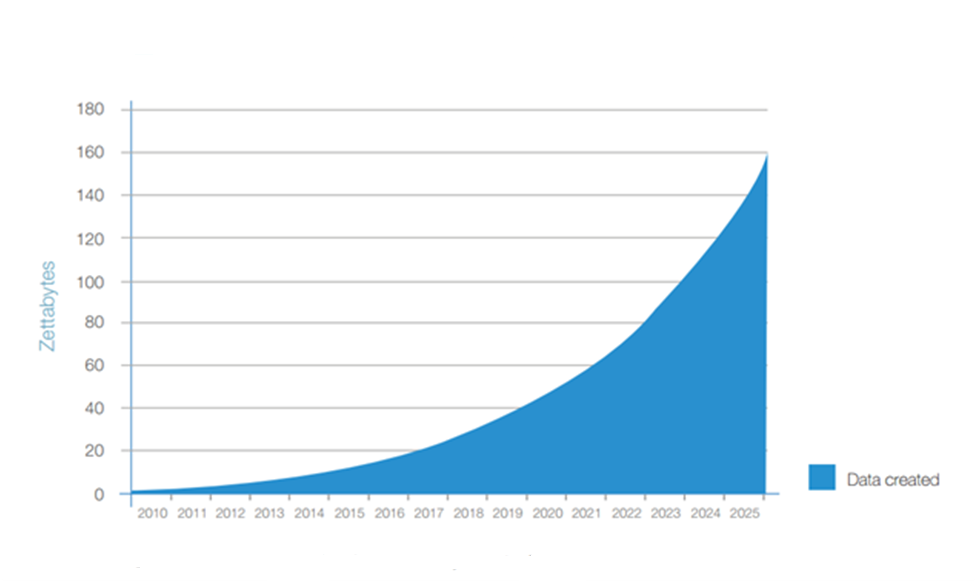 Exponential data growth trend from IDC study.
Serial links: Ethernet and 5G
The 400-Gigabit Ethernet (400 GbE) and 200-Gigabit Ethernet (200 GbE) are slated for official release by the IEEE P802.3cd Task Force in December 2017. Although the official IEEE roadmap has yet to precisely detail what lies beyond 400 GbE, doubling to 800 GbE will likely become a reality when single-lane 112-Gbps links hit the market.
This technology will allow larger lane bundles, providing 1-TbE or 1.6-TbE links with 10 or 16 lanes, respectively. Data centers maintained by Amazon, Facebook, and Google are moving to 100-GbE connections in 2017 and are expected to begin purchasing 400-GbE systems by 2019.
As such, it is critical for the current generation of 56-Gbps SerDes PHYs to meet the long-reach backplane requirements for the industry transition to 400-GbE applications. It allows the SerDes PHY designs to scale to speeds as fast as 112 Gbps, which are required in the networking and enterprise segments.
Take the case of enterprise server racks that are moving from 100 GbE to 400 GbE and beyond. Ethernet is moving faster than ever, and there is already a forum for 112-Gbps SerDes, which is going to be critical in driving the 800-GbE standard forward.
Supporting faster Ethernet speeds presents a distinct set of challenges for SerDes designers. In addition to maintaining signal integrity, engineers must contend with a stringent set of design requirements, such as architecting next-generation silicon within the same power envelope without the support of Dennard scaling.
Nevertheless, the industry is eyeing accelerated innovation to facilitate the transition from 28-Gbps to 56-Gbps to 100-Gbps single-lane.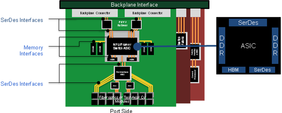 A view of network peripherals.
Regarding the wireless market, mobile operators and vendors have already embarked on R&D initiatives to develop 5G, which will be capable of supporting next-generation self-driving cars, UHD video, cloud robotics, 3D holographic telepresence, and remote surgery with haptic feedback.
The very first standardized deployments of the technology are expected to be commercialized by 2019 with the 3GPP’s initial 5G specifications slated to be implementation-ready by March 2018.
According to a new report by Research and Markets, the 5G network infrastructure market is projected to “aggressively grow” at a CAGR of nearly 70%, eventually accounting for $28 billion in annual spending by the end of 2025. These infrastructure investments will be accompanied by annual shipments of up to 520 million 5G-capable devices.
Perhaps not surprisingly, the impending shift to 5G has prompted wireless base station equipment manufacturers to design new architectures and systems to meet the design requirements by pushing high-speed interfaces like CPRI (to connect RF components) from 24G to 48G and JESD204 (to connect data converters) from 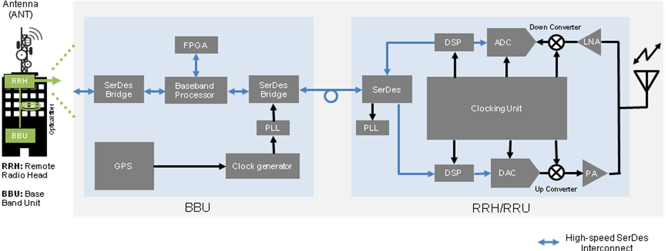 High-speed SerDes in 5G infrastructure.
With interconnect speeds fast approaching 56G and beyond, SerDes PHYs will play an important part in the development of wireline and wireless networking infrastructure. Therefore, system architects should carefully consider the pros and cons of design tradeoffs around die area and power.
Deciding on a specific set of tradeoffs for high-speed serial links may very well be one of the most complicated parts of the entire design process. It’s difficult to maximize operational efficiency and performance simultaneously.
Memory: DDR5 and HBM
Memory architecture is also evolving to meet the demand for increased bandwidth in both the wired and wireless markets. For example, JEDEC recently confirmed that its upcoming DDR5 memory standard will offer improved performance with greater power efficiency as compared to previous-generation DRAM technologies. The DDR5 specification will double the bandwidth and density over DDR4 along with delivering improved channel efficiency.
Meanwhile, high bandwidth memory (HBM)-based DRAM has been adopted for graphics, high-performance computing (HPC), server, networking, and client applications. As system designers look to move higher bandwidth closer to the CPU, HBM2 offers an opportunity to significantly expand memory capacity and maximize local DRAM storage for wider throughput in data center environments.
The HBM DRAM architecture increases system memory bandwidth by providing a wide interface of 1,024 bits to the SoC design. More specifically, second-gen HBM offers a maximum speed of 2 Gbps or a total bandwidth of 256 Gbytes/s. Although the bit rate is similar to DDR3 at 2.1 Gbps, the eight 128-bit channels provide HBM with approximately 15 times more bandwidth.
The HBM modules are connected to the SoC via a silicon or organic interposer. A short and controlled channel between the memory and the SoC requires less drive from the memory interface, thus reducing the power when compared to DIMM interfaces. Moreover, because the interface is wide, system designers can achieve very high bandwidth with a slower frequency.
As expected, the implementation of 2.5D technology in HBM2 systems adds numerous manufacturing complexities, requiring PHY vendors to work closely with multiple entities, including the foundry and packaging house. So a careful design of the entire system — including SoC, interposer, DRAM, and package — is essential to ensure high yield and proper system operation.
In addition, having a high-yielding module is a critical element of keeping costs in check, given the number of expensive components, including the SoC, multiple HBM die stacks, and the interposer. However, even with these challenges, the advantages of having increased memory bandwidth and density closer to the CPU clearly improves overall system efficiency for server and networking systems.
Acceleration: FPGAs and GPUs
Along with high-speed serial links and memory, GPUs and FPGAs have also played a significant role in helping to shape the modern data center. For instance, GPUs offer optimal performance, power efficiency, and compute density for many SIMD-style workloads with the use of a large number of processing pipelines that also support some amount of programmability.
First deployed in supercomputers and data centers for high-performance and scientific computing applications, GPUs have since achieved wider adoption as machine-learning applications have grown in popularity. Coupling a large number of parallel processing pipelines with the highest bandwidth memories, GPUs dramatically improve the time to train neural networks as they process training data at unmatched speeds.
For other types of workloads, FPGAs offer a more optimal solution than GPUs due to the broader flexibility and reconfigurability they enable to meet the varying demands of different applications. And while traditional CPUs offer the ability to run complete workloads of any type, FPGAs provide application-specific hardware acceleration and offload capabilities that can be updated over time.
Put simply, the flexibility afforded by FPGAs makes them a particularly powerful solution when paired with CPUs, allowing the benefits of general-purpose computation to be combined with those of hardware-accelerated processing for time-consuming and power-hungry tasks.
Advertisement
Learn more about Rambus Inc.


