BY DEBBIE SNIDERMAN
CEO, VI Ventures LLC
www.vivllc.com
The latest high-power silicon-based LED technology from Plessey Semiconductor is transforming form, function, and performance when it comes to luminaire design. Chip-on-board (COB) LEDs in a typical industrial luminaire are usually small, but the lens or reflector assembly and heat sink are much larger. New GaN-on-Si LED chip technology is changing it all, producing luminaire modules that are only 5.6 mm thick, including the optics. A single high-power GaN-on-Si chip can provide 30% more output through secondary optics than conventional four-chip solutions.
Silicon substrates are key to new designs
LEDs at Plessey Semiconductors are manufactured using GaN-on-Si substrates. Clive Beech, components manager, explains the many reasons why. “Silicon is a very good conductor of heat, making devices easier to heat-sink,” he says. “It’s economic and available in large quantities in many areas. Our factory has capability for CMOS processing on 6- and 8-inch-diameter wafers, a large advantage over sapphire substrates, which are traditionally and still run at 4 inches.”
“Silicon is also high-quality and available with low defect levels, and 6-inch substrates cost around one-tenth the price of 4-inch sapphire substrates,” he adds. “This gives us a lower-cost, high-performance LED compared to competitors, allowing us to put LEDs into new applications such as torches.”
The thermal performance in terms of thermal resistance is lower on silicon compared to SiC or sapphire substrates, so the thermal resistance from the junction LED surface-mounting point is lower. This allows Plessey to use higher surface-mount temperatures at the same junction temperature, which translates into having a smaller heat sink, saving space.
In addition to thermal and cost advantages, the surface of the silicon substrate offers another important advantage to Plessey’s LEDs. Sapphire emits light in all directions, so light from LED devices built on that substrate will emit not only from the surface but down the body of the LED as well, becoming absorbed. Silicon offers surface emission only, so vertical emission devices can be created with no absorption. It is possible to scale up the area of LEDs without losses in the bulk and even see performance improvements.
Another feature of using a silicon substrate is that multi-junction LED devices can be integrated with its circuitry on a single chip. This is a distinctive advantage for Plessey, who is the only one currently offering LEDs integrated with optics in the industry.
Changing luminaire design
Competitors use an array of smaller LEDs in their high-voltage packaged devices. For example, 12-V LEDs use four 3-V LEDs in series. With Plessey Semiconductor’s high-power multi-junction LEDs, the same lumen performance at the same current can be implemented with a single chip.
“This is a huge advantage in luminaires, especially in spot or other systems that use narrow beams,” says Beech. “When a luminaire has a device with four chips in a high-power package, they are traditionally put in a 2 x 2 array with no chip at the center. Putting this light through narrow-beam optics projects a crosshair in the middle onto a surface from the four chips. With a single chip and a single light-emitting surface, there is no crosshair pattern.”
The single monolithic high-voltage device produces a much better optical far-field image. It is also centered, being that the center of the emitting surface is at the center of the package. So there is also superior central beam candela power compared to a multi-chip solution. The peak intensity at the surface is greater than those that are not optically centered. “One customer uses our chip to produce a system with a beam angle of only two degrees,” says Beech. “Overall, the optics are better tuned to the emitting surface when a single chip is used.”
They especially help in narrow-beam systems like spotlights, portable lighting, flashlights, and 1,000-lumen tactical flashlights. Having a single, large emitting surface provides light that emits over long distances.
The new high-power LUCIAN PLW7070 single-chip LEDs can have larger chip dimensions compared to others produced on sapphire substrates and are used for portable torches and lamps, spot-lighting, down-lighting, high-bay, and floodlighting.
The operating life of Plessey’s GaN-on-Si LEDs have much better lumen maintenance. Competitor LEDs’ light output degrades 7% to 10% over 6,000–7,000 hours, while theirs only reduces by 3% over the same time.
New process for creating pre-focused LEDs
Plessey Semiconductors’ patented Stellar LED manufacturing process was developed in 2015. It involves patterning GaN devices on a silicon substrate and mounting a second silicon substrate on top, then flipping the entire structure over and removing the back side to reveal a new substrate. This allows holes to be etched in the substrate that reach the LED below, effectively creating LEDs that are layered and sandwiched between two substrates.
The most important feature of this process is the ability to create micro-mirrors that pre-focus the light coming out of the LED at the chip level as part of the LED processing. The process doesn’t remove certain areas from one of the substrates and fills the holes to form the micro-mirror. The end result is that the LED produces inherently narrow beams that don’t require secondary optics. The pre-focused narrow-beam LED system saves money, size, and the need for additional optics and can become much smaller and less expensive in time.
New reflector designs: COB arrays with micro-reflectors
Plessey’s Stellar Orion LED beam-forming module is a COB version of these integrated optics for directional lighting applications that Beech says has won several awards. Normally, a 15- or 16-degree spotlight would have a large reflector and a mirror on the front surface, but theirs doesn’t need them. Instead, it uses an array of micro-reflectors around each of the LEDs. The spotlight’s total thickness, including the integrated reflectors, is 7 to 8 mm thick, the same as the diameter of the reflector and much smaller than other technologies.
Some spotlight applications require a cover plate for environmental protection, but there is no lens. The optics are designed and built into the unit itself. Integrating the optics into the LED system itself is unique in the industry, and currently, Plessey Semiconductors is the only one offering this advantage. Samples of its Stellar Orion product are currently shipping with a range of 25- and 60-degree beam angles.
“These are now our standard product and are more attractive and look less industrial than the typical spotlights they are replacing,” says Beech. It is a stepping stone toward a fully integrated solution in which the LEDs have built-in collimated beams and will be much smaller, anticipated to be available in the next year or so. At that point, the micro-reflectors wouldn’t be needed, and the total thickness of the devices integrated into the LED chip itself would be on the order of a few hundred microns. “The current standard product is like an analog version of what’s coming at a much larger scale,” he says.
Evolving heat sinks
In devices with space constraints, such as down lights, small heat sinks are important. High-power LEDs are similar to other power devices: Power goes in, light and heat come out. For a given level of heat generated, the thermal path is key to what the junction temperature will be.
As a starting point for designing the heat sink, it must not exceed a 135°C junction temperature. At the maximum operating current, given the low thermal resistance of the substrate, the solder-point temperature at which the device is mounted to the circuit board will be about 20 degrees below that, or about 115°C.
“We face our heat sinks to the outside air,” says Beech. “The thermal resistance of the heat sink to the ambient environment is a strong function of the specific design and surface area. Because we run at higher solder-point temperatures, we can use smaller heat sinks and still have good performance.”
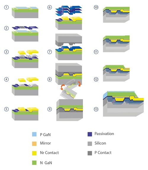
Plessey’s patented high-power LED manufacturing flow schematic.
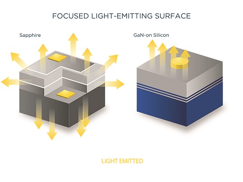
Silicon acts as a mirror reflecting light out of the top of the device. With sapphire substrates, some light is inevitably lost inside the substrate.
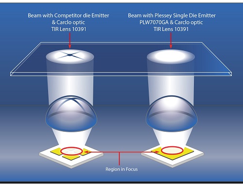
Using a single monolithic die eliminates the cross-hairs often visible on competing multi-chip products.
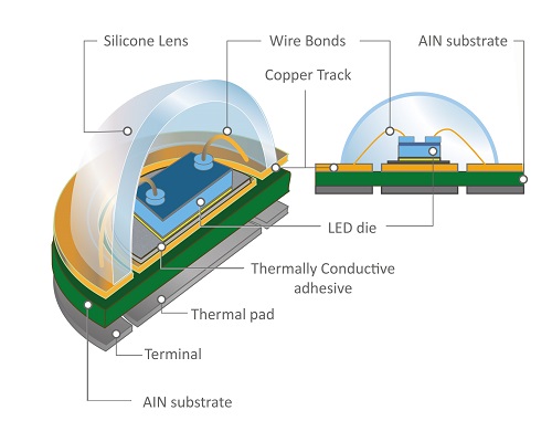
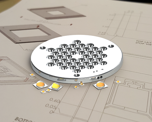
A packaged Plessey multi-junction GaN-on-silicon device.
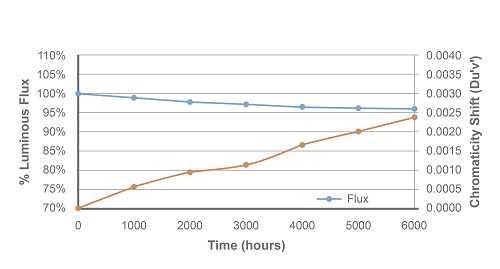
Luminous flux maintenance and color shift over 6,000 hours (LM-80 assessment) measured with worst-case conditions of Tsolderpoint = 105°C and IFmax = 1.25 A. The orange line shows very good color stability over the stress period for GaN/Si.

Yesterday versus today.
Stellar ORION product.
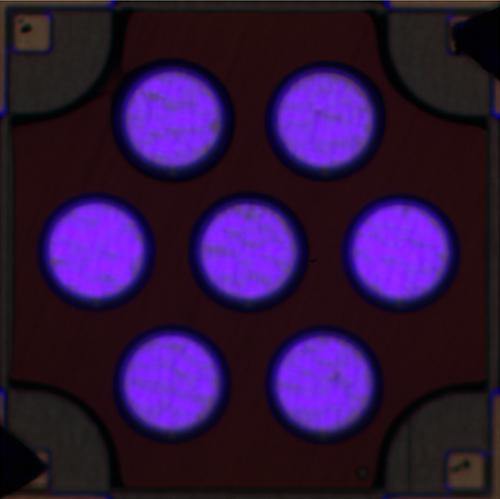
The 7070 Multi-junction.
On-chip optics.
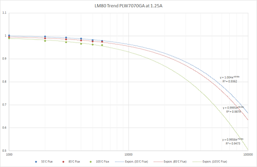
The latest LM-80 chart for Plessey’s PLW7070 showing lumen depreciation.
Advertisement


