BY TED MARENA, Director of FPGA/SoC Marketing
Microsemi Corp.
www.microsemi.com
Communications, industrial, and even embedded designs increasingly require higher-performance interfaces. Protocols such as DDR4 memory, 10 Gigabit Ethernet, PCIe, serial ADC and DAC interfaces, and others are becoming commonplace. While these higher-speed interfaces are usually found on high-end FPGAs, this is often an overkill approach and cost-prohibitive for most applications. And using low-end FPGAs is not an option because they do not provide the necessary performance.
Now the cost of deploying these interfaces can be dramatically reduced using a new class of energy-efficient, mid-range-density FPGAs that are cost-optimized, consume lower power, and offer smaller form factors than more expensive FPGAs while still delivering generous high-speed interface options.
Addressing new market dynamics
Although individual market segments are unique, they also share several characteristics. The requirements for better value and lower cost are growing drivers for all applications and market segments. In addition, faster and numerous networking interfaces are now more common given the emergence of the Internet of Things (IoT). Finally, high-speed processing in most embedded designs is a new norm.
These factors require architectures that incorporate interfaces such as Gigabit Ethernet, along with transceivers fast enough for 10 GbE, JESD204B ADC/DAC, PCIe interfaces, HDMI 2.0b and memory buses such as DDR4, to name a few.
Now that these types of interfaces are available in cost-optimized, low-power mid-range FPGAs, design engineers have important new options for addressing the latest market dynamics for their products. Among the most valuable of these options is the ability to use Serial Gigabit Media Independent Interface (SGMII) on the FPGA’s generic general-purpose input-output (GPIO) pins rather than having to use high-speed transceivers.
Leveraging SGMII on GPIOs
The most common interface being leveraged in many communications and industrial designs is Gigabit Ethernet (GbE). Most frequently, an FPGA connects to a PHY via a serial SGMII interface. In the past, using FPGAs to implement an SGMII interface also required using high-speed transceivers. This all changes with the availability of new cost-optimized mid-range FPGAs, which make SGMII interfaces available on generic GPIO pins for the lowest-power implementation possible for GbE links to an FPGA.
Many embedded product developers use GbE for an increasing number of connections. No longer only for data payloads, these links are becoming ubiquitous for control, management, status, and more. While both low-end and traditional mid-range FPGAs can support these 1-Gbps speeds, they require transceivers to implement the 1.25-Gbps SGMII interfaces as well as other high-speed interfaces. Ideally, a device would have generic I/O pins assigned specifically to support SGMII (Fig. 1 ).
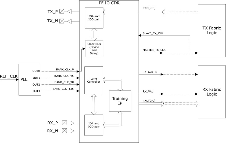
Fig. 1: Traditional and mid-range FPGAs can support 1-Gbps speeds, but they require transceivers to implement the 1.25-Gbps SGMII interfaces.
Low-end FPGAs and traditional mid-range FPGAs do not have this feature, so they must rely on transceivers. Implementing interfaces in this way can be challenging because these transceiver interfaces are precious and frequently scarce. To have enough of them to meet higher-performance interface requirements, designers previously had to select a more expensive, higher-density FPGA fabric.
These large FPGA fabrics are often not required in industrial designs, but designers were forced to choose them anyway just to have enough additional transceivers. In addition, these larger devices mean that larger package form factors are required. The result is higher power consumption and costs in industrial markets that need just the opposite.
Today’s lower-power, cost-optimized mid-range density FPGAs buck these trends, offering a new way to meet the requirement for numerous Gigabit Ethernet links via SGMII on GPIOs. Some solutions go a step further to incorporate a clock and data recovery (CDR) circuit into high-speed LVDS I/Os that can support 1.25 Gbps. These features allow the device to support SGMII interfaces on numerous GPIO pins. Using this architecture, designers can reduce the cost, size, and power of their designs as compared to those created using traditional mid-range or high-end FPGAs.
Balancing speed, cost, and power
Not every design with communication interfaces requires extremely high performance, but across the markets, processing needs are increasing while interfaces are getting faster. These factors require FPGAs to support serial interfaces of up to 12.5 Gbps to implement the following increasingly common options:
- PCIe Gen2 requiring 5 Gbps
- HDMI 2.0b, which needs 6 Gbps
- 10 GbE requiring 10 Gbps
- JESD204B, which can run up to 12.5 Gbps
These high-speed serial interfaces require transceivers to operate up to the speeds listed above, but power consumption should also be optimized. The performance for these rates is trivial for high-end FPGAs or mid-range FPGAs built off of high-end architectures. Unfortunately, these devices also consume very high power, require large form factors, and are often beyond the budget for many designs.
On the other hand, low-density FPGAs often do not have transceivers, and those that incorporate them do not support the performance rates listed. The answer to balancing transceiver speed, low cost, and power efficiency is to use mid-range density FPGAs with the right mix of logic elements (LEs) and transceivers to support the required data rates.
With these kinds of options, industrial architects can support the latest high-speed serial interfaces while also having adequate LEs on-chip to implement necessary board functions. In addition, the ability to implement SGMII on GPIOs as well as transceivers often enables designers to select smaller package sizes and densities. This lowers system costs and reduces the power needed for FPGA functionality.
One example where serial interfaces are required is for a wireless microcell. These designs typically use a processor to handle most of the signal processing while leveraging an FPGA for custom signal conditioning and to connect to the ADC and DAC, as shown in Fig. 2 .
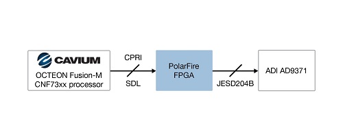
Fig. 2: Example of a serial interface design.
In this example, the FPGA uses transceivers to implement either CPRI or a proprietary serial digital link (SDL) to the Cavium processor and a serial link to Analog Devices’ ADC/DAC via JESD204B. In addition to performing the serial bridging functions, the FPGA’s fabric can implement signal conditioning algorithms such as crest factor reduction (CFR) and other functions. This implementation provides a lower-power solution and a smaller footprint for small cell and microcell applications.
A new way to implement DDR4 interfaces
The most common memory that engineers tend to connect to an FPGA is DDR DRAM-based devices. There are several generations to choose from, and the best choice is generally to use memory that has been shipping for some time and is not the absolute newest standard.
For DRAMs, DDR4 offers the best cost per bit, and its architecture will be supported for numerous years. Although DDR3 is still a viable choice for designs, DDR4 is being selected for the majority of new designs because it will offer reduced pricing in the future, faster performance, and wider single-chip data buses.
There were no low-density FPGAs that supported DDR4 memory interfaces, so designers had to use mid-range density FPGAs that were built off of high-end architectures to implement these interfaces. In contrast, today’s latest mid-range FPGAs are purpose-built for these interfaces, offering the required DDR4 performance at significantly lower cost and power while enabling the much smaller form factors required for embedded designs (Fig. 3 ). Package sizes for these devices range from 16 x 16 mm down to 11 x 11 mm.
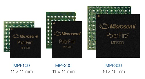
Fig. 3: FPGAs in multiple densities and form factors.
With growing demand for higher-performance interfaces, more connectivity, and lower costs for communications, industrial, and embedded designs, system architects and engineers need to look for new solutions. Today’s lower-power, mid-range density FPGAs solve these design challenges, combining greater value with lower power consumption while still providing the interface options and other capabilities demanded by modern designs.
Advertisement
Learn more about Microsemi


