By MICHAEL HORNKAMP,
Sr Director High Power Regional Marketing and Application Engineering,
Power Integrations
www.power.com
IGBTs are used to switch power in many products such as variable frequency drives (VFDs), servo drives, electric cars, buses and trucks, trains, medical equipment (x-ray and MR) , air-conditioners and even some professional audio systems. These are all termed ‘high power’ applications, which may lead them to be considered more electrical than electronic and therefore less sensitive. However, there are still a number of different failure mechanisms which will result in the destruction of the IGBT unless great care is taken during system design and operation.
Like all devices, operating conditions – temperature, thermal shock, thermal and power cycling and vibration – can cause failure. ESD, too, can be a killer, but and we often see failures due to poor handling practices, possibly because IGBTs and gate drivers are often installed by cabinet installers rather than electronics personnel. Protecting IGBTs against these types of failure is largely a matter of following installation guidelines and ensuring that the device is being held within its defined operating conditions.
Overcurrent is another potential cause of failure. There are integrated solutions to this problem, but there are also simple, low cost solutions using measurements made by the current transducer in the AC output, so most customers prefer not to pay for the extra protection.
The main other failure mechanisms are short circuits, high di/dt, high dv/dt and gate-emitter and collector-emitter over-voltages. It is these types of failure that industry demands protection against – especially as power levels approach 100 kW and beyond and systems become expensive – so manufacturers of IGBT drivers such as Power Integrations have built-in innovative and reliable protection regimes into their products that address these circumstances to safeguard the IGBT module.
Short circuit
Figure 1 shows the behavior of an IGBT under two different short circuit conditions with low inductance (case 1) and high inductance (case 2). One commonly-used method to detect short circuits, and therefore turn off the IGBT before it is damaged is to use an optocoupler IC with integrated ‘desat’ (desaturation) protection. Unfortunately, there are two disadvantages. Firstly, optocoupler ICs with desat protection also require high voltage diodes which can be expensive and lossy. Secondly, and perhaps more importantly, the required desat monitoring electronics are often too sensitive to EMI or VCE voltage spikes. This can result in false short circuit identification, causing the IGBT to turn off for no good reason. A different method is employed by Power Integrations in its IGBT-drivers which use an ASIC chipset to reduce component count and size, and increase performance, efficiency and scalability. The chipset also includes advanced monitoring and controlling features. To address short circuit measurement, the SCALE-2 chipset and a resistor chain are used to dynamically measure the VCE of the IGBT (see Fig. 2 ). Not only does this mean that small spikes do not cause false triggering, but also there are other advantages. The resistor chain method is lower cost than the standard diode measurement option, and has no coupling capacitance. Therefore there is no additional efficiency-sapping capacitance and no negative effects due to dv/dt. A further advantage is that the sensitivity of the devices can be easily adjusted to suit the particular application using a reference pin.
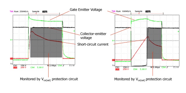
Fig. 1: IGBT behaviour with low inductance (Case 1); and high inductance (Case 2)
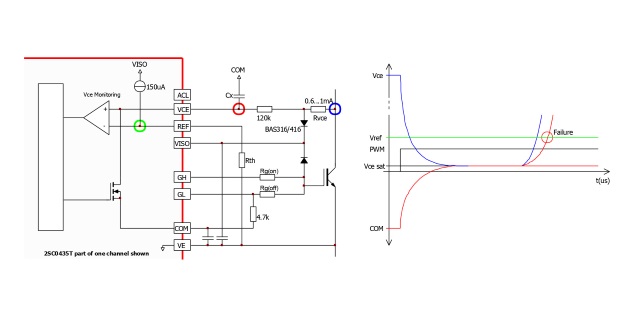
Fig. 2: To address short circuit measurement, the SCALE-2 chipset and a resistor chain are used to dynamically measure the VCE of the IGBT
Advanced and dynamic advanced active clamping
The SCALE-2 chipset is also used to implement sophisticated Active Clamping techniques to address other IGBT failure modes mentioned earlier – high di/dt, high dv/dt and gate-emitter and collector-emitter over-voltages.
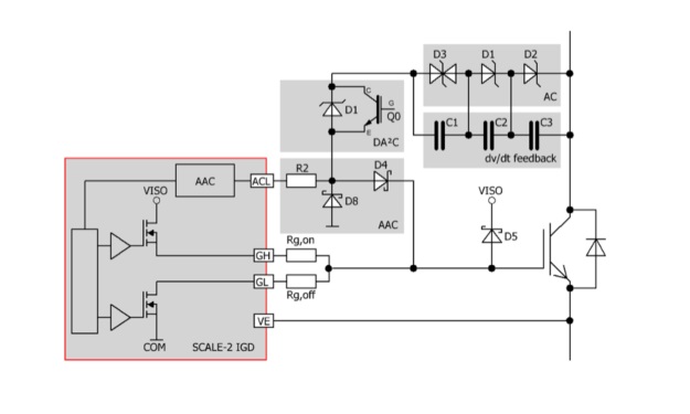
Fig. 3: Dynamic Advanced Active Clamping with dv/dt feedback
Basic active clamping (AC box in Fig. 3) limits the IGBT’s VCE during turn-off. The IGBT is partially turned on as soon as its VCE voltage exceeds a predefined threshold. The IGBT is then maintained in linear operation which reduces the rate at which the collector current falls, thereby restricting the collector-emitter over-voltage. With SCALE-2 technology, Advanced Active Clamping (AAC) feedback (box AC and AAC in Fig. 3) operates on the driver’s secondary side ASIC. As soon as the voltage increases due to the active clamping activity, the turn-off MOSFET of the driver connected to GL is progressively switched off. This reduces the charge that flows from the IGBT gate to COM through the turn-off gate resistor Rg,off. As well as reducing the IGBT turn-off collector-emitter over-voltage this cuts power losses in the TVS, improving efficiency.
A dv/dt feedback function (box dv/dv feedback in Fig. 3) can also be implemented in SCALE-2 drivers. This results in very efficient turn-off over-voltage limitation during regular switching operation without thermally overloading the TVS diodes. During the collector-emitter voltage rise, a currentflows in the capacitors and is applied parallel to the TVS diodes. This current further supports the Advanced Active Clamping, because it flows to the same driver’s terminal, but is applied sequentially prior to the Advanced Active Clamping feedback. With this additional driving method, the VCE voltage clamping is more effective and the losses generated in the TVS are reduced. If set up correctly, the IGBT can work continuously in this operational mode. Therefore, it is possible to switch an IGBT module with higher dc-link stray inductance without exceeding the module’s Reverse Bias Safe Operating Area (RBSOA). Also, snubber capacitors may not be necessary.
Power Integrations has taken clamping one stage further: Dynamic Advanced Active Clamping (DA2 C) adds an additional TVS diode(s) (box DA2 C in Fig. 3 ) in series with the TVS diodes used for Advanced Active Clamping. This additional TVS diode is short-circuited with an auxiliary switch Q0 during the IGBT on-state as well as for about 15 to 20 µs after the IGBT turn-off command to guarantee efficient active clamping (the additional TVS diode is not active during IGBT turn-off). After this delay, the auxiliary switch Q0 is turned-off. The additional TVS diode is therefore activated and allows the DC-link voltage to be increased to a higher value during the IGBT off-state. This means that the output inductors of the converter system can be demagnetized after emergency shut-down, avoiding a short but otherwise inevitable DC-link voltage increase.
Soft shut down
Both AAC and DA2 C suit applications with high commutation stray inductances that require the control of IGBT turn-off di/dt, and make operation possible within the reverse bias safe operating area. But some applications, for example with low commutation stray inductances and where the IGBT turn-off overshoot falls within the RBSOA, a simpler option is Soft Shut Down (SSD), which has the advantage of not requiring TVS diodes to perform the active clamping. SSD is activated after a short-circuit is detected. It protects the IGBT against destruction by limiting the short circuit duration and current slope in order to keep momentary VCE below VCES (IGBT blocking voltage capability). Figure 4 shows the principle of the SSD function.
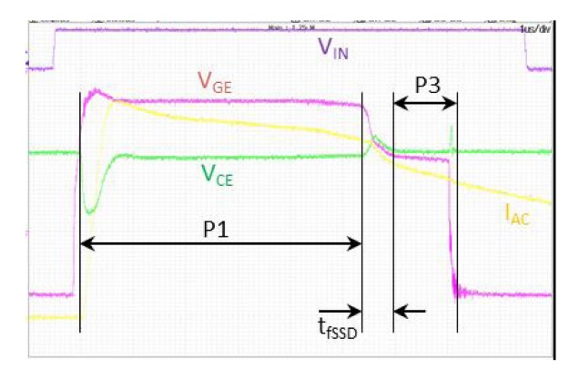
Fig. 4: The soft shut down principle shown on a scope
The VCE desaturation is visible during time period P1 (green line) and thanks to the rail-to-rail gate driver output stage technology, the VGE (gate-emitter voltage, pink line) is kept very stable. After P1 (approximately 5 µs), VGE is limited to a lower value during a period specified as tFSSD . During tFSSD , the short circuit current IC is limited and initially a small overvoltage VCE occurs. During time period P3, the gate of the IGBT is being further discharged. Shortly before the discharging process is finished the gate-emitter is connected to COM. The remainder of the gate charge is removed, the short circuit current is switched off and a second small VCE overvoltage occurs. The whole short -circuit current detection and safe switch-off is lower than 10 µs. Power Integrations enables this through a version of its SCALE-2 technology, SCALE-2+ which enables either AAC / DA2 C or SSD to be implemented.
Integration
At the heart of all the IGBT protection schemes described here, is Power Integrations’ SCALE-2 chipset, which adds these functions to its main task of driving, controlling and monitoring the performance of the IGBT module. The chipset mops up a significant number of passive and active components that other solutions require to complete these functions. In this way not only do the products deliver increased functionality, they also improve reliability and decrease size.
Advertisement
Learn more about Power Integrations


