By Tim Dhuyvetter, senior principal member of the technical staff, Mobile Solutions, Maxim Integrated
Most touchscreen panels have a limited type of haptic feedback or none at all. This is also true for many types of handheld or wearable devices like watches, touchpads, keyboards, a mouse, etc. The desire for improved haptic feedback is leading some to take a closer look at piezo transducers to generate haptic signals, which provide a number of physical and electrical improvements over traditional vibration generators.
This article reviews piezo transducer principles, theory, and modelling. It includes a discussion of electronic circuits that are specifically designed to drive the unique characteristics of piezo transducers and shares examples of haptic applications using piezoelectric transducers. The article also examines the relationship of amplifier input power with respect to piezo load configurations.
Note that haptic vibration from piezo actuators uses the inverse piezo effect (i.e., vibration from electrical stimulus). Any mention of piezo effects refers to this electrical-to-mechanical energy transfer.
Introduction to piezoelectric haptics
Today, in most handheld or portable electronic devices, a haptic vibration is created by an electromechanical (EM) transducer that converts electrical signals into mechanical vibrations. These include eccentric rotating mass (ERM) actuators and linear resonant actuators (LRAs). These types of EM transducers are low-cost, are fairly easy to use, and can be powered from a battery-level voltage.
There are, however, a number of disadvantages to EM transducers:
- They are resonating devices that create a specific vibration frequency and, in the case of an LRA, it must be calibrated to a resonant frequency that is stochastic from the factory.
- EM devices are physically large and tall (3 to 5 mm high), reducing the ability to mount them into thin enclosures.
- They produce point-source vibrations and cannot create various frequency patterns onto a surface.
- They are inefficient, requiring significant energy per haptic event.
- LRA devices are somewhat fragile and can be destroyed by either physical or electrical overstress (e.g., a drop).
In comparison, piezo transducers are not based on EM energy conversion and excel as a haptic vibration generator. They generate mechanical vibrations though the inverse piezo effect by creating crystalline vibrations from applied electromotive force (i.e., EMF), typically from an AC voltage source.
Piezo transducers can be advantageous due to several important properties:
- They are thin ( <1 mm), are flexible, and can be mounted in a variety of options and shaped to nearly any desired pattern.
- They produce vibrations over a surface area and can be touch-location–sensitive.
- They are highly efficient, depending on the method used to drive the piezo.
- They can reproduce any vibration frequency over a wide frequency range.
- They can generate a pattern of haptic signals that can be amplitude- or frequency-modulated.
- They have very little inertia and, therefore, have a very fast response time.
- They produce no EMI emissions.
Note that piezo actuators require a relatively high voltage-drive signal to create significant mechanical vibration, typically 60 V to 200 V peak to peak. Also, piezo actuators are primarily a capacitive load to the drive circuit and, therefore, benefit from specialized electronic drive circuitry. More on this subject will be discussed later.
A detailed discussion of piezo actuator construction and physics is beyond the scope of this paper; however, a brief description follows. Piezo transducers are manufactured in a variety of different physical configurations, depending on the application. A piezo actuator that is most generally used for haptic and audio reproduction takes the form of a bimorph bender that would be mounted (i.e., glued) to an internal surface that is part of a handheld or wearable case or a touchscreen, for instance. An example of a single-layer piezo actuator that is surface-mounted is shown in Fig. 1 .
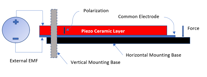
Fig. 1: Bimorph piezo actuator construction
As shown in Fig. 1 , a bimorph bender is generally composed of one or more layers of polycrystalline ceramic material screened onto a conductive, mechanical layer (e.g., brass or copper). After the layers have been created, a large DC polarizing voltage is applied across the piezo structure to align the crystal domain boundaries to strengthen the inverse piezo-effect force that will be generated (i.e., increasing force generated per voltage EMF). The polarizing voltage then defines the direction of the mechanical force generated with applied voltage. Increasing applied voltage in the direction of the polarizing voltage increases the mechanical force or bending displacement. Polarization to the piezo layers can be applied in the same direction or in opposite directions. Each method has its advantages and can be used to create piezo effects as desired.
The illustration in Fig. 1 shows a piezo actuator mounted to a surface that is orthogonal to the polarizing voltage. This configuration (with the applied EMF as shown) generates a force into the mounting base, and consequently, there is little deflection of the piezo. If the base was mounted vertically to the piezo actuator (shown in dotted lines) and the opposite end of the actuator was unconstrained, this would cause a larger deflection of the piezo.
An example of the mounting shown in Fig. 1 would be to a display screen generating a force that is conducted to a surface. This creates maximum conductive force and minimum deflection. This method could be used, for example, in generating a haptic vibration to fingers on a touch-activated display screen. It should be noted that any material that is present between the piezo and the mounting surface absorbs mechanical energy and tends to attenuate the conducted vibration, especially if the material is soft or pliable.
A piezo transducer can also be used to provide localized haptic feedback. This can be accomplished by arranging a number of piezo elements under a touchscreen or keyboard display, for example, so that each piezo element provides a haptic feel localized to its placement. When a touch is sensed, not only does the display produce the X-Y location of the touch, but a piezo driver is enabled that energizes that particular piezo actuator. This can be accomplished by using a high-voltage MUX or from separate piezo amplifiers.
Each layer of polycrystalline ceramic produces a force proportional to the applied voltage, and n-layers produce n times the force generated.

Piezo materials are subject to various aging or degrading effects that can be catastrophic or cumulative. Temperature, humidity, and pressure can cause long-term damage and lifetime degradation to the strength of the piezo effect. Hermetically sealing the piezo actuator reduces humidity effects, and normal atmospheric pressures have limited aging effects. The primary causes for piezo age degradation are high temperature and continuous DC bias.
Voltage overstress is similar to voltage breakdown and can be catastrophic. If a piezo actuator is subjected to differential voltages in excess of the polarization voltage, the piezo ceramic will return to its original randomized crystalline structure and the piezo effect will be greatly reduced. Similarly, if a piezo is subjected to temperatures beyond its Curie point, the crystal structure will again be randomized. Both DC bias and exposure to high temperature cause cumulative degradation of piezo effect. Polarization of piezo material is shown in Fig. 2 .
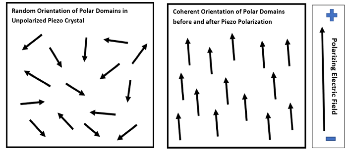
Fig: 2. Piezo actuator showing polycrystalline domains before and after polarization
Recommended
Piezo haptic driver extends battery life in portables
Piezo modelling and resonance
As mentioned previously, the electrical model of a piezo actuator can be primarily a capacitor with series resistance. This is a useful simplification for circuit modelling, but it is not strictly true. In fact, measuring a piezo with a network analyzer reveals that there are several electrical resonant frequencies occurring at approximately octave multiples of the primary resonant frequency. For example, if the primary electrical resonance occurs at 8 to 9 kHz for a particular piezo, there will be additional resonant points at 34 KHz and 83 KHz. This has been observed in the lab but might be true only for that specific piezo element. The key point to keep in mind, however, is that the electrical resonance is independent from the mechanical resonance, and mechanical resonance is far more useful and important than electrical resonance for haptic applications.
For example, the same bimorph piezo actuator mentioned above, mounted in an edge clamp, shows a mechanical resonance at approximately 300 Hz (observed with a laser deflection measurement system) and has a capacitance of 400 nF. Therefore, the electrical resonance frequency is 30× higher than the mechanical resonance and, as will be shown, has little effect to the driving amplifier. It is also important to note that mechanical resonance is dependent on the mounting method and the mass of the mount. The final mechanical resonance value will, therefore, have several stochastic variables such as mounting, mass, and factory variations.
Piezo capacitance, which represents the amount of stored charge in the piezo, is also complicated. Consider a piezo drive signal that is a continuous sine wave centered at the mechanical resonance frequency. Because the current in a capacitor lags the voltage across it by 90°, the charging current in a piezo peaks at the –6-dB value of peak applied voltage (or, in general, at the maximum slew rate of VOUT ). Therefore, the reactive power needed to charge a piezo peaks at this same voltage point.
It is also interesting to note that (low-frequency) piezo capacitance is not a fixed value; it has first- and second-order voltage coefficients. For example, in some piezo transducers, capacitance peaks at an applied voltage lower than its rated value. Obviously, this makes exact electrical piezo modelling difficult. Fortunately, a single capacitance plus series resistance is sufficient for most haptic applications that require only low-bandwidth signal response. It is interesting to note that the electrical energy required to drive a piezo actuator (similar to the one described in this article) does not change significantly at the mechanical resonance frequency, except that charging energy is linear with frequency, as will be discussed below.
For haptic applications, closed-loop bandwidth requirements are generally low (i.e., 3 to 5 kHz is generally sufficient). Also note that at DC, the applied voltage on the piezo is static and no vibration is created. Because the electrical load is primarily capacitive (with electrical resonant points), piezo charging current continues to increase with increasing frequency until ESR dominates and the piezo is electrically resistive.
Fig. 3 shows a measured plot of piezo impedance frequency sweep. Figs. 4 and 5 show an electrical model and simulated piezo frequency sweep, respectively. The series LRC networks are configured to match the measured electrical frequency resonance points at 8 kHz, 34 kHz, and 80 kHz, each of which have low Q. C1 and R1 represent the low-frequency capacitance and series resistance of the piezo and dominate the load presented to the amplifier output.
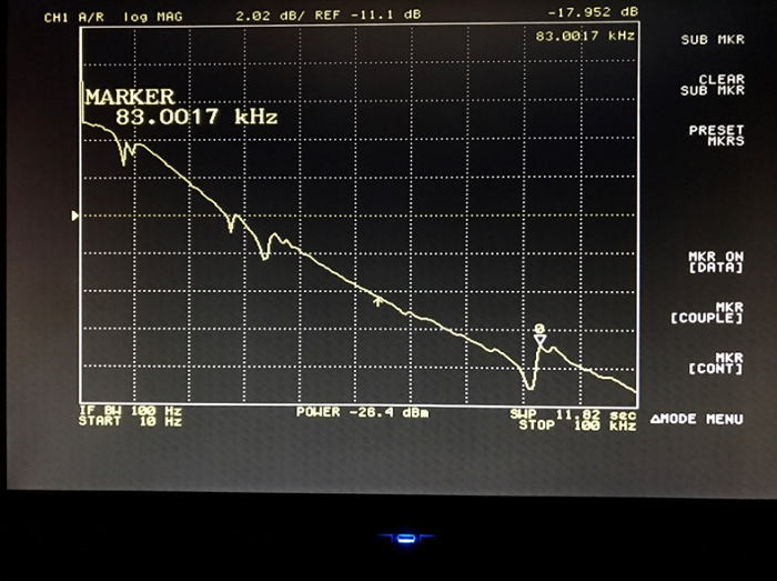
Fig. 3: Frequency response of piezo actuator with network analyzer
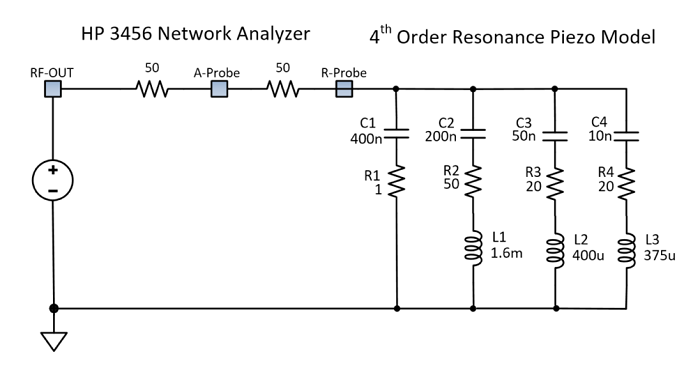 Fig. 4: Matching electrical model
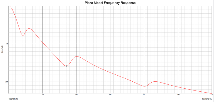
Fig. 5: Piezo model frequency response simulation
Piezo charging and energy requirements
Most haptic signals are based on sine or Gaussian waveforms. The waveforms can repeat and form a tone-burst–type envelope or can be single-pulse events. They can also be constructed of amplitude-modulated envelope shapes or can be composed of frequency-modulated tone bursts or any combination. The nearly unlimited haptic shapes can be used to create any desired haptic “feel.” The simplest haptic waveforms are used as simple alert or touch feedback response. Also, because haptic waveforms are essentially audio waveforms, the sound of a haptic signal from a piezo actuator can be used to enhance the response.
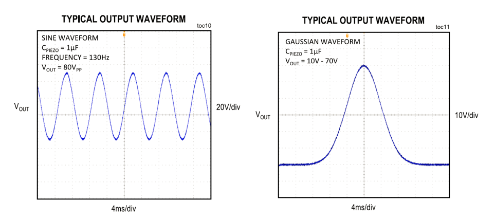
Fig. 6: Examples of typical haptic waveforms (6a: sinewave; 6b: Gaussian)
The energy required to charge a capacitor (piezo) with a sine wave is proportional to frequency, voltage, and capacitance as follows:
P(reactive) is proportional to: 2pi × C × V2 × F
From the equation above, the independent variables of C, V, and F determine the amount of energy required to drive a piezo. For a haptic waveform signal driving a specific piezo actuator, the capacitance and frequency are generally fixed for that application. For example, typical haptic frequency is between 100 and 300 Hz, and piezo actuators range from 100 nF to over 1 µF (depending on the number of ceramic layers and size). The dependent variable left is voltage swing. Based on piezo ceramic thickness and type of ceramic used, the maximum peak voltage is set. As previously mentioned, the polarization voltage must not be exceeded.
Commonly available piezo actuators have rated maximum voltage ranging from 30 to 200 V. These values are only typical values; new piezo materials and construction techniques are constantly being developed, especially as a result of new application demands and use cases.
Presently, however, the capacitive nature of piezo materials and the need to drive high-voltage waveforms dictate the charging energy needs and the type of electronic circuits used to drive piezo elements. Due to the capacitive nature of a piezo load, a Norton-based (current output) drive circuit is the most appropriate.
The differential equation form of capacitor voltage as a result of charging current is:
dV = (dI/C)dT (incremental capacitor voltage is proportional to integration of charging current X time)
and Q = CV (total charge on a capacitor is proportional to capacitance X voltage on capacitor)
Then dQ = dI × dT (the incremental stored charge is proportional to the integration of charging current through time)
Most prior art piezo drive circuits use a traditional boost converter to generate a high-voltage rail that powers a voltage-output linear amplifier (i.e., a low-impedance output amplifier). This concept is shown in Fig. 7.
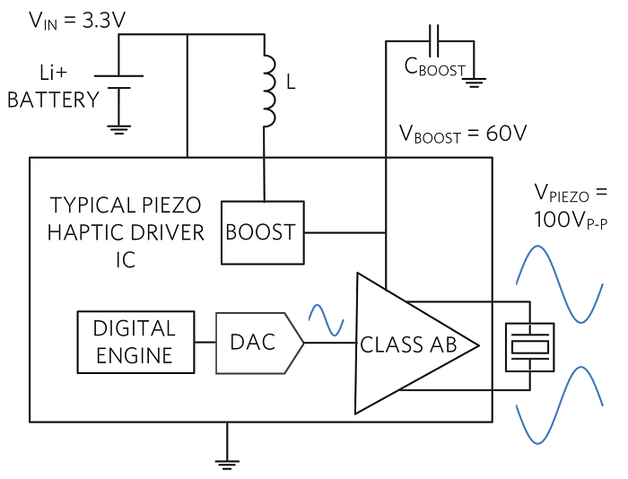
Fig. 7: Prior art piezo driver circuit with boost converter and Class A/B amplifier
There are several drawbacks to the piezo driver topology shown in Fig. 7 , primarily related to input power consumption and IC power dissipation. By inspection, there are two power conversion stages, each with their own power efficiency loss. First, there is a boost converter that is used to generate a high-voltage DC supply rail that is used by the differential output amplifier. Typical boost converter efficiency for a high conversion ratio, high-voltage supply is perhaps 70% to 85%. The second power converter is the output amplifier that differentially drives the piezo actuator. In this embodiment, the piezo load driver is a linear amplifier (i.e., Class A/B) that typically is 50% to 67% efficient.
The product of the two efficiencies results in 35% to 57% total efficiency. Note that there is no real output load power (the load is capacitive); therefore, all input power is dissipated across the IC. For example, with large piezo capacitance (>1 µF), high voltage swing (> 100 Vpp), and high haptic frequency (~300 Hz), input power becomes excessive and the IC will heat up significantly and likely go into thermal limiting.
It is interesting to consider that the Class A/B amplifier in the topology above can be replaced with a Class D amplifier, resulting in a much higher driver efficiency. However, a low-resistance inductor will be required in series with the piezo load to attenuate the Class D modulating frequency carrier from dissipating in the piezo.
Piezo charging and energy recovery
To reduce power loss and to alleviate the power dissipation issue, energy recovery can be used to recover the energy used to charge the piezo capacitance and pass it back to the input supply or intermediate storage capacitor. Using this method, most of the reactive energy is recovered from the piezo and input power is greatly reduced. It is possible to achieve close to a 10× energy ratio compared to the energy loss in the topology shown in Fig. 7 .
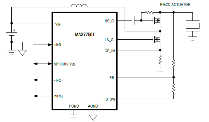
Fig. 8: Piezo driver IC with energy recovery
The schematic shown in Fig. 8 is a simplified block diagram of Maxim’s MAX77501 piezo haptic actuator boost driver. It is configured as a single-end output driver/controller with external power FETs designed to provide a high degree of application flexibility. The MAX77501 is built in a 12-V, BiCMOS process with 10-V gate drive outputs. Playback of haptic signals can be generated from streaming data (SPI interface) or can be stored in 9 kB of internal RAM. A 12-bit DAC and buffer amplifier complete the digital engine signal path. The input supply range is 2.8 to 5.5 V, and the boost amplifier typically drives piezo loads up to 120-V peak and up to 2-µF capacitance. Other digital functionality includes enable, FIFO fill status, and a system interrupt request (nIRQ) due to fault conditions.
The principles of energy recovery or energy recycling are illustrated the waveform plot shown in Fig. 9 . The upper plot (in blue) is a sinewave haptic signal that is measured across a piezo actuator (80 V peak to peak at 250 Hz). The lower plot shows the input supply current measured at the battery output (3.6 V). During positive dV/dT slope of VOUT , energy from the battery is required to charge the piezo capacitance and battery current is positive (i.e., >0). Note that, as mentioned earlier, the input current peaks at the max VOUT dV/dT or lagging VOUT by 90°. During negative dV/dT slope conditions, energy from the piezo needs to be removed to reduce VOUT incrementally in time and the input supply current is now negative (i.e., the battery supply is absorbing energy transferred backward into the battery).
A plot of VBATTERY is not shown here, but depending on the driving point resistance of the battery, VBATTERY voltage will be observed to rise and fall as the supply current goes forward or backward. At the peak or valley regions where VOUT has no slope (i.e., dV/dT is zero), the input supply current is near zero. By this method, energy is used to charge the piezo and then recycled (or recovered) when the charge is removed. There are energy losses, of course; power is consumed by real power loss elements (e.g., switch, metal, and inductor DCR) during both directions of energy transfer, which leads to an overall efficiency loss per complete cycle of the haptic signal. For example, if the power loss per cycle is 20%, then there is an 8:1 efficiency improvement compared to not using energy recycling. Referring back to Fig. 7 , it can be seen that the linear amplifier takes energy from the boost converter output to charge the piezo capacitance during both positive d(VOUT )/dT) phases. The amplifier output then must discharge the energy stored in the piezo to ground during negative d(VOUT )/dT phases. Discharging the energy stored in the piezo causes the input power to increase dramatically, most of which is dissipated across the IC.
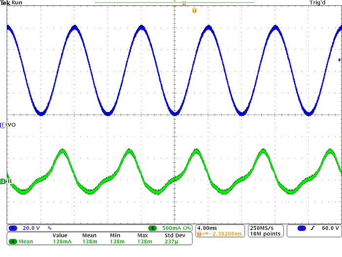
Fig. 9: Scope shot of piezo haptic output waveform (blue) with input current plot (green)
Summary
Piezo transducers have a number of unique attributes that make them highly suitable for generating haptic feedback vibrations. This article reviewed typical piezo transducer construction techniques along with electrical and mechanical modeling. It also discussed safe operating area, piezo degradation, and aging effect issues and provided examples of electrical drive circuits to address the specific requirements of piezo elements as well as application examples.
In addition, the article shared a proprietary energy recovery process that greatly reduces input power requirements, thus allowing the driver IC to handle much larger piezo capacitance/voltage actuators without exceeding junction temperatures associated with piezo driver ICs that use a linear amplifier driver.
Advertisement
Learn more about Electronic Products MagazineMaxim Integrated


