Do you see that grumpy old engineer in the corner of the lab who delights in sending new graduates down to stores to get a bag of holes? That could have been me, but when personnel departments became Orwellian Human Resource departments banning you from taking leave during Team-Building Days, I decided to leave employment and start my own company. Freedom? Well, of a sort — you do still need to produce things that might sell. But you do get to spend a few days exploring some dimly lit avenue of electronics without having marketing asking you to produce yet another PowerPoint presentation for management that tries to justify their inspired idea that breaks a fundamental law of physics. This article is about one such diversion.
I enjoy reading the articles of those eccentric engineers emulating past microprocessors such as the 68000 or even a Cray. My own favorite processor was the Motorola 6809, and I used it as a workhorse in my early days as an engineer, using an old Dragon home computer as a development tool. I was thinking of designing it into an FPGA — just for fun — when a more pressing need took hold.
I used FPGAs a lot in my designs and usually needed a processor for some housekeeping or control purpose. Although FPGA-based processors were available, such as Altera’s Nios, they did use quite of lot of resources and often required external code memory, encumbered as they were by C compilers and even operating systems. I decided to design my own minimal microprocessor for those simple tasks such as I2 C control of peripherals or simple control interfaces such as digital encoders and character LCD displays. I loosely based the design on my favorite, the 6809, but soon started stripping it bare, finally managing to squeeze a workable processor into less than 400 logic elements (LEs — basically a four-input look-up table followed by a programmable flip-flop — the building blocks of FPGAs), allowing it to fit in the smallest of FPGAs or allow multiple instantiations in the same FPGA.
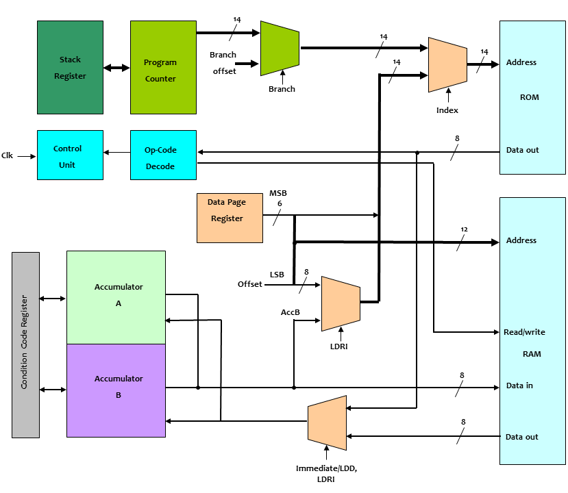
The block diagram of the processor, which I call the PT13, is shown in Fig. 1 .

Read the full article on EDN.
Advertisement
Learn more about Electronic Products Magazine


