How to optimize the gate drive design for high-voltage MOSFETs
Properly designing the gate drive circuit for high-voltage MOSFETs is essential to ensure the best performance
BY ALEXANDER CRAIG
Fairchild Semiconductor, San Jose, CA
http://www.fairchildsemi.com
Properly designing the gate drive circuit for high-voltage MOSFETs is essential to ensure proper performance from the MOSFET one desires. Far too often, engineers find themselves having difficulty in power loss or noise generation and blame the MOSFETs, when in fact they need to take a closer look at how they’re driving the MOSFETs.
New technologies such as charged-balance devices have dramatically reduced the RDS(on) for specific die size MOSFETs and packaging. They’ve also improved the gate charge of the MOSFETs, which prevents these high-voltage devices from handling more current and from switching faster. However, in order to do this properly one needs to design the gate drive correctly, in addition to paying careful attention to layout.
This paper will provide the basic tools for selecting the correct gate drive and gate resistance and also point out where to look for information on the datasheets for critical pieces of information needed. It will also provide some unique equations that are not typically seen in power electronics. Power dissipation, “Pd ” consists of the conduction losses and the switching losses of the device which can be calculated with Equation 1.
P d = D* R DS(on) *I D2 + fsw*(E on +E off )
Equation 1
The conduction losses represented by the first term are straightforward, where D is the duty cycle, ID is the drain current and RDS(on) is the resistance drain to source. The second-half of the power dissipation equation has to do with switching losses. The way this is written is typically seen in reference to IGBTs, but the fsw *(Eon +Eoff ) is much more descriptive of sources for the switching losses. Depending on the circuit, there may be no or very low turn-on losses “Eon ” or turn-off losses “Eoff .”
For MOSFETs, these losses are influenced by the MOSFET switching speed and recovering diode which may be a body diode of a MOSFET. When a diode recovers a high current, the “Irrm ” is seen in addition to the expected ID used in the conduction loss calculation.
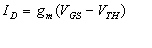
Since a MOSFET can operate in the “linear mode” at certain Vg , ID conditions allow it to act as a current limiter and not as a switch. It is possible, with a poorly designed gate drive, that at turn-on and into a reverse recovering diode the MOSFET will experience a point in the linear mode and this will cause a higher junction temperature.
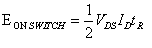
Finally, these losses are multiplied by the switching frequency (fsw ). To properly design the gate drive circuit one needs to take into account the Qg , Vplato , Vdd of the gate drive and Rg both internal and external. The EON loss attributable to the switch alone with no diode recovery can be calculated by Equation 2. Here VDS is the off-state drain-to-source voltage and ID is the drain current, so the MOSFET, seen just after the turn-on event, where tR is the rise time is controlled by the gate drive design.
Equation 2
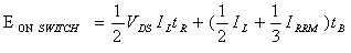
The additional EON loss including the diode recovery can be calculated by Equation 3 in which IRRM and tB are properties of the recovering diode.
Equation 3
From the above equations it is clear that the faster the MOSFET is turned on (smaller tR ) the lower the EON will be, but a few factors limit the turn-on speed. These factors typically include the layout and parasitic drain inductance which causes noise, ringing and gate drive current capability.
To best explain the design procedure it helps to use a simple low-side gate drive circuit and focus on the turn-on event but it should also be understood that the same considerations apply to turn-off as well and to a high-side driver. All MOS controlled devices have a gate charge curve in their data sheet that looks like Fig. 1 .
Some points to consider are VTH at the end of t1 the Vp , or plateau voltage, at the end of t2 and the cp , the point at which the MOSFET channel is fully enhanced. During interval t1 IG increases quickly and charges the combination of CGS and CGD to the gate threshold voltage VTH through. In this interval the MOSFET channel has not been established and therefore carries no current.
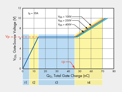
Fig. 1. Gate charge curve for MOS-controlled device.
As interval t2 begins, the MOSFET starts to conduct current in the linear mode in which the MOSFET is not fully on, and therefore sees a high voltage and a high current. This is a very wasteful power mode. In this mode, think of the MOSFET as acting like an amplifier in which
The parallel combination of CGD and CGS are charged from the VTH to a plateau level given by
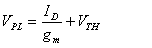
As the drain current rises from zero to ID . The charge needed during this transition from the gate drive can be determined from the MOSFET datasheet gate charge curve. QGt2 , the charge at the beginning of the plateau region with the end of t2 , allows us to calculate either the time or current required for this transition
Throughout t2 VDS remains high. At the end of t2 the MOSFET conducts the full load current. The peak current delivered from the gate drive circuit occurs during this time and can be derived as
There are two limiting factors for the peak gate current, one is Rg the other is the gate drive circuitry. For a short period of time the gate drive may be limiting the output current, and will have a voltage drop of Vdd –Vg . This is a power loss mode, which one needs to be aware of. The drain current rises from zero to the operational current as the gate drive voltage goes from VTH to Vp . But VDS remains high and we are still in a high-power loss mode for the MOSFET.
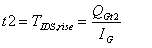
The above is quite detailed and gets us to the point of the beginning of t3 , the plateau region. For a very short period of time the peak drain current can be higher than required during the plateau region. Since t3 is typically much longer, t1 + t2 for most applications, a simpler first order approximation can be used. If one wants a MOSFET to be fully switched on with any given rise time, the gate drive must supply a gate current defined by Equation 4 where Qg(cp ) is the amount of charge required to fully turn on the MOSFET.
IG(req) = Qg(cp) /tR
Equation 4
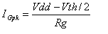
So if we want a tR of 10 ns with the FCP20N60 we need to supply a Qg(cp) of ~45 nC from the gate charge curve below. We need a Gate drive capable of delivering an IG on 4.5 A from equation 4.
Since we now know the required gate drive current IG(req) to the turn-on and a desired speed, we now need to design a gate drive circuit to deliver the IG(req) . Figure 2 depicts the basic low side driver for a boost circuit take note of VDD, RG and IG. The first factor in gate drive selection is to ensure that the selected gate drive device can deliver the IG(req). The second step helps understanding where the IG is derived. Once the MOSFET is in the plateau region, the voltage available to charge the gate is VDD-Vp. So if the VDD available is 12 V the voltage available to derive IG is ~5.8 V. With this we can calculate the maximum Rg from RG(max) = (VDD Vp )/IG(req) therefore our example is RG(max) = 5.8 V/4.5 A = 1.29 Ω. This represents the total RG and should include the internal gate resistance on the MOSFET.
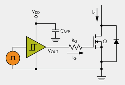
Fig. 2. Depicts the basic low side driver for a boost circuit.
In some applications, an asymmetrical gate drive is desired in order to have different turn-on and different turn-off speeds. A typical implementation of this is shown in Fig. 3a where Ron and Don make up the charging path while Roff and Doff make up the discharging path. One needs to take the VF on the diodes into account when calculating the resistance needed.
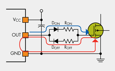
Fig. 3a. An asymmetrical gate drive to get different turn-on and different turn-off speeds.
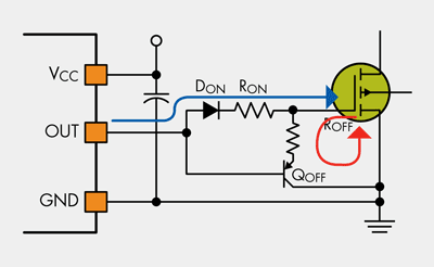
Fig. 3b. Circuit that offers a slow turn-on and a fast turn-off
In some cases a turn-on mau needs to be slow but the turn-off needs to be as fast as possible, so for these cases the circuit in Fig. 3b is a good solution. The turn-on is once again controlled by Ron and Don but the Roff and Qoff control the turn-off and should the Gate drive IC not be able to sink the desired fast turn-off current the Qoff and Roff can. It must be noted that in order to enable fast turn-off one should keep the loop created by the MOSFET gate-drain capacitance, Roff and Qoff as small as possible. ■
Advertisement
Learn more about Fairchild Semiconductor


