By Filadelfo Fusillo, LV Power Transistors & GaN senior application development engineer, and Filippo Scrimizzi, LV Power Transistors & GaN application development manager, STMicroelectronics, www.st.com
Modern power conversion requires ever-increasing efficiency combined with high power density. In fact, making a small high-efficiency system means saving space and reducing energy consumption, which are key factors in applications such as auxiliary DC/DC converters for hybrid electric vehicles (HEVs) and full electric vehicles (EVs), high-end switch-mode power supplies (SMPS) mounted in high-power servers, and high-end UHD flat-panel televisions.
However, high efficiency and high power density are not easy to attain because some design choices can achieve one target (i.e., power density) but worsen another one (i.e., efficiency). This is why selecting a suitable system topology and semiconductor devices is so important.
To improve the trade-offs, one strategy is to use soft-switching converters, which guarantees minimization of switching losses, low EMI, and high power density. In this article, we focus on two different application segments — auxiliary DC/DC converters for HEVs/EVs and high-end SMPS for cloud and servers — and use an ST low-voltage power MOSFET for synchronous rectification as an example.
Using soft-switching converters and synchronous rectification to improve performance
In the traditional SMPS, during turn-on and turn-off transients, semiconductor devices sustain hard switching transitions with high switching losses that are especially evident in high-power and high-voltage applications. Resonant converters represent an interesting option for applications requiring high power density, high reliability, and high efficiency. Generally, resonant converters are switching converters that include a resonant circuit (a combination of inductors and capacitors) that actively participates in determining the power flow from input to output. They process power in a sinusoidal way, and the power switches are softly commutated. Depending on the combination of reactive components (inductors and capacitors), resonant converters can be classified as three major types: series , parallel , or series-parallel .
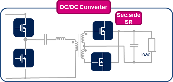
Fig. 1: LLC converter schematic.
Among all of the resonant converters, the LLC converter (Fig. 1 ) is probably the most common topology (medium power range) in the power supply environment with some clear advantages (high efficiency, zero-voltage switching [ZVS] capability even at no load, and good output voltage control at all load and line conditions). In an LLC converter, primary-side transistors serve as half-bridge switches while the resonant capacitor, resonant inductor, and magnetizing inductance form the LLC resonant tank. At the secondary side, the synchronous devices rectify the square wave across the transformer to create the desired output voltage.
Compared with traditional PWM converters, LLC topologies achieve both high efficiency and wide input voltage range capability. ZVS at the primary side can easily be achieved for the entire load range. For higher power, phase-shifted full-bridge topology with ZVS (PSFB-ZVS) becomes very popular and common in power supply design ([1], [2], [3]). This converter is frequently used to step-down high DC voltage, providing electrical isolation. It is commonly used in server and telecom SMPS, renewable energy systems, and battery-charging circuits.
Four semiconductor devices (MOSFETs or IGBTs) at the primary side in full-bridge configuration form a PSFB converter, while at the secondary side, diodes or power MOSFETs act as synchronous rectifiers (Fig. 2 ).

Fig. 2: PSFB-ZVS full-bridge converter schematic.
The primary-side MOSFETs are arranged in two legs: right leg (Q1-Q3) and left leg (Q2-Q4). These two legs commutate with a short shift time, also called phase shift (Fig. 3 , left side). By phase-shifting the two legs, signal modulation and the control of the power delivered to the secondary side are obtained.
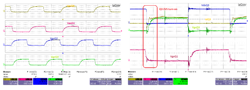
Fig. 3: Q1-Q2-Q3-Q4 gate signals at no load (left), ZVS turn-on waveforms (right).
Zero-voltage switching is obtained by a resonant discharge of the output capacitance of the primary switches; the body-drain diode of each MOSFET conducts before the MOSFET itself, ensuring the device turn-on with negligible drain-source voltage drop. In this way, ZVS operation helps reduce switching losses and device stresses (in this topology, there are no snubber circuits).
In Fig. 3 (right side), the turn-on waveforms for the Q3 device are depicted: Here, Q3 output capacitance is discharged by the primary resonant inductance, then the current commutates into the Q3 body diode (VDS ≈ 0 V), and finally, Q3 is turned on and the current starts to flow in the device channel. Therefore, turn-on losses of the primary switches become negligible, improving the converter’s efficiency.
In both topologies, when the output current and power increase, further efficiency improvement can be achieved only by an optimal design of the synchronous rectification stage and judicious choice of semiconductor devices. Therefore, the secondary-side synchronous rectification realized by using low-voltage power MOSFETs is the best way to boost system efficiency, thus allowing both high frequency and reduced volume. MOSFETs replace power diodes (or Schottky diodes), used in low-power converters; as VDSon F . MOSFETs are the preferred choice at high output currents because of their low conduction losses.
Low-voltage MOSFET technology has developed rapidly to meet the increasingly challenging application requirements (power losses, efficiency, and switching speed). Nowadays, low- and medium-voltage devices are mainly realized using trench-gate layout, which guarantees better performance than old planar structures. In a trench device, the gate structure is formed inside the epitaxial layer; this structure shows lower specific on-state drain-source resistance (RDSon,sp ) due to the absence of JFET resistance.
In fact, as shown in Fig. 4 , the trench extends beyond the P-base region limit, connecting N+ and N– regions. The absence of the JFET region and the cell-pitch reduction minimize the device-specific RDSon [4]. State-of-the-art trench technologies ensure excellent performance not only during on-state (low RDSon and conduction losses) but also during switching transients because of low Qg that minimizes switching and gate drive losses. The modern trench technologies have consequently improved Figure of Merit (FOM = RDSon * Qg ).
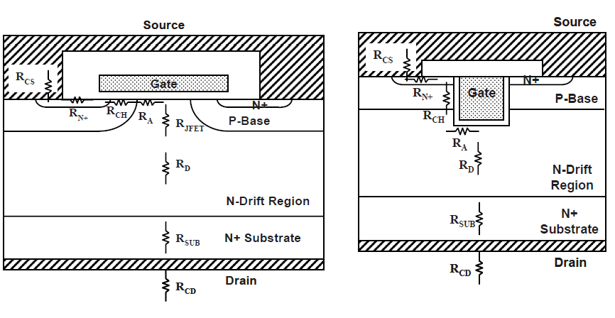
Fig. 4: Planar and trench structures’ section.
In synchronous rectification, the major power MOSFET losses are the following [5]:
1. Conduction losses
2. Body-drain diode recovery losses
3. Output capacitance losses
4. Driving losses
Conduction losses are given by the following formula:

where IRMS is the rms value of the drain current.
Clearly, conduction losses become very important in low-voltage and high-current platforms, so synchronous rectifiers must be chosen in an optimal way: Both silicon and package features must guarantee very good performance at high output currents. Very low-RDSon devices assembled in SMD power packages (i.e., H2PAK) or low-profile (PowerFLAT 5×6) packages will minimize the conduction losses.
During the dead time, the current flows through the MOSFET body diode, which is forward-biased. The diode conduction losses are represented by this formula:

Diode losses are proportional to output current, switching frequency, forward voltage drop, and dead time. Minimum dead time can be useful to reduce diode conduction losses. When the body diode conducts, a minority charge is stored on both sides of the p-n junction. At turn-off, these stored charges must be removed before the device can sustain voltage, as shown in the following:

where Qrr is the body diode reverse recovery charge.
MOSFETs with low Qrr and soft recovery optimize diode recovery losses and improve the device performance in terms of voltage spike and EMI.
During the reverse recovery process, together with the removal of the excess stored charge, the MOSFET output capacitance must be charged to the secondary-side transformer voltage (VS ) to sustain off-state voltage. When the reverse current reaches its peak, the output capacitance is fully charged to the transformer voltage.

This capacitive loss is particularly significant at no or light load conditions.
The gate driving losses are the power losses related to the MOSFET turn-on and -off. While at high current levels, the conduction losses prevail in the system power management, and at light load conditions, the driving losses can become even more important. The driving losses are quantified as:

As shown by this formula, the higher the fSW , the bigger the driving losses. Switching frequency and gate driving voltage are design parameters, while QG is the only parameter related to the device choice. Power MOSFETs with low QG are best to minimize the gate drive losses, especially at light load conditions in high-frequency converters.
MOSFET switching losses (during turn-on and turn-off transients) are negligible in synchronous rectification because the device commutation happens in ZVS condition. In fact, the secondary current flows through the body diode (VDS = –0.7 V) before the channel conduction. In this way, the MOSFET commutates with very low voltage across it, and the switching losses are negligible.
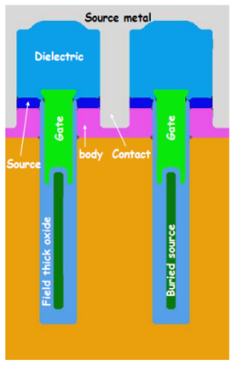
Fig. 5: Shield gate trench structure cross-section.
The values of RDSon , Qrr , and Qg (only at light load or at very high fSW values) are the key parameters for enhancing the overall performance of synchronous rectifiers and, therefore, of the entire system. Modern MOSFET technologies show excellent performance in on-state not only because of their lower specific RDSon (RDSon *A) but also their dynamic behavior, with significant reduction in QG and Qrr . For example, ST’s shield gate trench MOSFET technology has the above-mentioned features and represents an optimal choice for synchronous rectification in high-power converters (Fig. 5 ).
Auxiliary DC/DC converters for HEVs/EVs
Carmakers have been developing alternative-fuel vehicles in response to the public’s increasing concern about pollution, climatic changes, and global warming. The limits on the emissions of combustion engines become narrower and narrower, so HEVs and EVs are gaining market share in the automotive engine scenario. In HEVs, two distinct types of power are used for propulsion (typically, a gasoline engine with an electric motor), while EVs use one or more electric motors for propulsion. Fig. 6 represents a simplified scheme of a full electric vehicle.
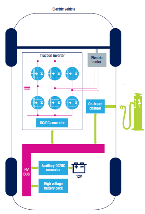
Fig. 6: EV architecture.
A high-voltage bus connects the high-voltage battery pack to the traction inverter for car motion and other inverters, including those for power steering and air-conditioning, for example. The auxiliary DC/DC converter can step-down the high-voltage battery level to a low-voltage battery value (typically, 12 V or 24 V).
A low-voltage battery is required in modern cars because a large number of loads are fed at the 12-V level such as head- and taillights, audio and multimedia systems, heating fans, and so on. Bidirectional converters can operate in both modes: step-down — charging 12 V from an HV bus — and step-up (boost) — converting 12 V to an HV battery value. And because transferring energy between these two battery packs is an intelligent and convenient solution, the auxiliary DC/DC converter design becomes the key step for an optimized energy transfer and battery management.
The typical power rating for an auxiliary DC/DC converter in HEVs is in the order of some kW. Because the common battery level for a low-voltage pack is 12 V, the output current range is very high (200–250 A). So it becomes mandatory to maximize the converter efficiency, higher than 90% for new projects, to improve battery management as well as the performance of the entire system. In addition, higher switching frequencies reduce the size of passive components (transformers and filters), improving the size and weight of the converter.
However, because switching losses increase with the switching frequency, the topology choice becomes crucial to meet these targets. Soft switching techniques such as ZVS and zero-current switching, among others, are the best solutions for attaining high power density, high efficiency, and low switching noise. For our experimental test, the test vehicle is a ZVS full-bridge phase-shifted converter (see Fig. 2 ) with the following features:
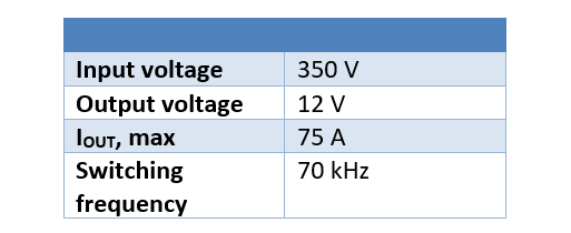
Table 1: PSFB-ZVS full-bridge converter features.
In the topology described above, the primary FETs switch in zero-voltage conditions, meaning that the body-drain diode of each MOSFET conducts before the MOSFET itself, ensuring the device turn-on with negligible drain-source voltage drop. Therefore, the turn-on losses are zero, reducing the device switching losses. The right silicon technology for primary side devices must be selected following these considerations:
a) Figure of Merit (FOM = RDSon * QG ) should be as low as possible for high-voltage devices. In fact, low RDSon considerably reduces the conduction losses ( ), which become greater at high load currents, while low QG ensures fast turn-off switching and reduced gate drive losses ( ;
b) High threshold voltage (VTH ) helps reduce switching transitions at turn-off, minimizing the turn-off losses, while at turn-on, it improves the device immunity against switching noise;
c) MOSFET output capacitance (COSS ) should be as low as possible to extend the ZVS range and reduce dead time. In fact, at no or light load conditions, ZVS may be lost if the inductive energy is not enough to swing the output capacitances of the two FETs in the same leg of the bridge and the transformer. Low COSS values reduce the capacitive energy related to the FETs and transformer, enlarging the ZVS range. Moreover, the lower the COSS , the shorter the dead time, which enhances system performance especially at high frequency;
d) Body-drain diode must be robust with fast recovery process [5].
To target these specifications, some companies have developed dedicated technologies for ZVS converters. For example, STMicroelectronics has the DM2 and DM6 (MDmesh), which are already automotive-grade–qualified. The DM6 is obtained as a further development of DM2 technology, achieving very good performance thanks to lower switching losses and extremely low reverse recovery time (trr ) and charge (Qrr ) (Fig. 7 ).

Fig. 7: DM2 vs. DM6 switching losses (left) and DM6 diode reverse recovery process (right).
In synchronous rectification, the best choice is a 100-V low-RDSon , low-Qrr power MOSFET. In the following table, we show the main electrical parameters of two 100-V power MOSFETs (STripFET F7 technology as compared to planar technology). The two devices have the same die size.

Table 2: SR FETs electrical parameters.
The switching performance of SR FETs can be evaluated by the analysis of the device waveforms at full load (75 A) in terms of voltage spikes and gate voltage integrity. In our tests, no dangerous spike and gate voltage spurious ringing is detected (shown in Fig. 8 are the relevant waveforms for our example 100-V device). Then the impact of the selected SR FETs on system power management is given by efficiency and power losses calculation.
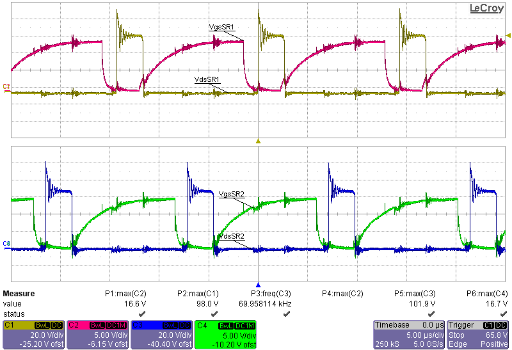
Fig. 8: 100-V STripFET F7 SR FETs waveforms @ 75 A.
As shown in Fig. 9 , this device shows better performance in efficiency, both at light and at full load, which is linked to lower values of RDSon and Qrr and, as a consequence, lower conduction and diode losses.
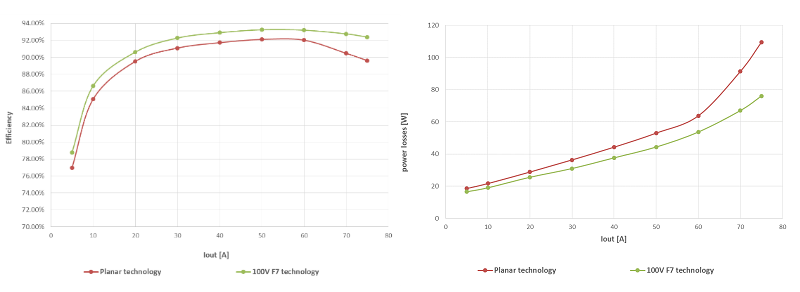
Fig. 9: Efficiency and power losses comparison.
The 100-V power MOSFETs show excellent efficiency in the complete current range, thus representing a good choice for secondary-side synchronous rectification thanks to its overall performance.
High-end SMPS for server and cloud computing
Digital information management continues gaining importance in our economy: Data centers, storage, and networking are crucial in several economy sectors. However, because the latest data centers require ever-growing power as well as temperature management, “energy savings” is the mantra among power system designers. In fact, smaller and higher-efficiency systems mean lower power consumption and optimized size.
For these reasons, designers of high-end power supplies choose resonant topologies with low-voltage MOSFET synchronous rectification to maximize system efficiency and power density. From medium to high output power ( DSon power MOSFETs used as synchronous rectifiers. In particular, Table 3 shows the main electrical parameters of two 100-V devices; one that guarantees very low RDSon and Qrr , two parameters that are very important in synchronous rectification. These devices are compared in a 500-W LLC DC/DC converter with digital control (VOUT = 12 V, IOUT = 42 A).

Table 3: 100-V SR FET electrical parameters.
MOSFET breakdown voltage must be chosen in the right way, ensuring a good safety margin against an undesired drain-source voltage spike when the load current is zero (Fig. 10 ).
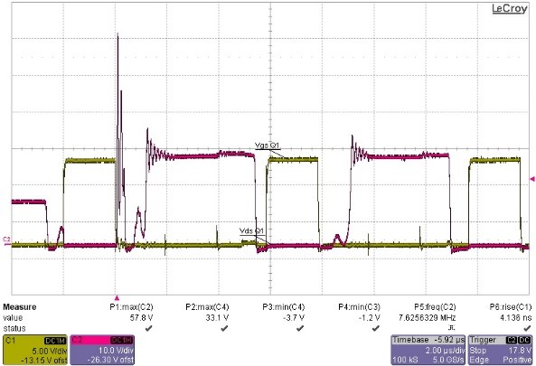
Fig. 10: Drain-source voltage spike at no load in a 500-W LLC DC/DC converter.
At full load, our example device (Fig. 11 ) shows better switching performance, having superior immunity to spurious turn-on and showing excellent EMI performance.
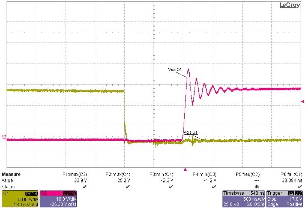
Fig. 11: 100-V STripFET F7 turn-off waveforms in 500-W LLC DC/DC converter.
Finally, the efficiency is obtained by measuring the input and the output power for each current step (after reaching the thermal steady state) (Fig. 12 ). Our example 100-V device shows higher performance both in switching and in efficiency, an optimal choice for secondary-side synchronous rectification in high-end SMPS.
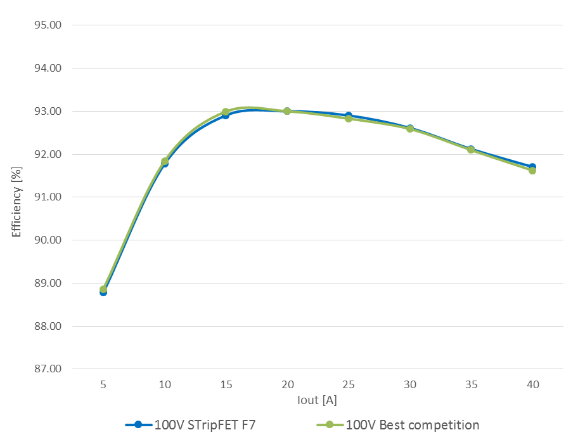
Fig. 12: Efficiency comparison.
Conclusion
High efficiency and power density are the main requirements in high-performance power converters, such as auxiliary DC/DC converters for HEVs/EVs and high-end SMPS for server and cloud applications. System design and device selection must be optimized to achieve the best efficiency target. 100-V STripFET F7 technology shows excellent overall performance, representing the best solution for low-voltage MOSFETs in synchronous rectification.
References
[1] Chuan-Sheng Liu, Liang-Rui Chen, B.Z.Li, Z.P.Huang, “The implementation of a full-bridge phase shifted zero-voltage switching power converter”, PEDS2009.
[2] C.D.Davidson, “Zero voltage switching full-bridge converter topology”, in Proc. IEEE INTELEC ‘10, 2010.
[3] B.Yang, J.L.Duarte,W.Li, K.Yin, X.He, Y. Deng, “Phase-shifted full bridge converter featuring ZVS over the full load range”.
[4] B. J. Baliga, “Fundamentals of power semiconductor devices”, Springer, 2008.
[5] L.Hua, J.Guo, X.Jing, S.Luo, “Design considerations for secondary side synchronous rectifier MOSFETs in phase shifted full bridge converter”.
Advertisement
Learn more about Electronic Products Magazine


