HVICs for robust energy-efficient motion control
The latest drivers ease energy-saving-design difficulty
BY HENNING HAUENSTEIN
International Rectifier
El Segundo, CA
http://www.irf.com
High-voltage ICs that meet power-semiconductor-gate-drive requirements are increasingly deployed in the inverter stages of energy-efficient motion-control designs. Providing high levels of integration, these HVICs allow engineers to quickly meet energy-saving design requirements while minimizing component count.
The latest high-speed power MOSFET and IGBT drivers, for instance, require neither a clamping diode nor limiting resistor and offer optional dependent or independent high- and low-side-referenced output channels with a gate drive supply range from 10 to 20 V. The output drivers from the IRS260xD family, for example, feature a high-pulse-current buffer stage with minimum driver cross-conduction.
The floating channel can be used to drive n-channel power MOSFETs or IGBTs in the high-side configuration operating up to 600 V. The devices provide matched propagation delay for both channels and an advanced input filter to improve noise immunity. Negative voltage spike immunity protects the system during high-current switching and short circuit conditions.
In addition to the undervoltage lockout functionality provided by many gate driver ICs, the new motion control-oriented families feature a very low quiescent current, enabling the use of a bootstrap power supply for even the most demanding applications. To reduce component count still further and make the design even easier and more reliable, the latest drivers even integrate the bootstrap function. This is implemented with an internal high-voltage MOSFET to deliver current to the high-side circuit through the low-side supply network (emulating the external high-voltage bootstrap diode).
For a successful inverter application, an HVIC must deliver suitable performance in both normal operation and at potential operational extremes. The ability to handle negative transients is particularly important.
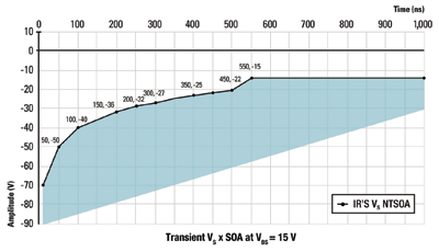
To meet this requirement, manufacturers have created a method for characterizing and specifying gate driver capability with respect to handling negative transients. This method uses the concept of negative transient safe operating area (NTSOA).

Fig. 1. Negative VS transient SOA for HV gate driver ICs (at VBS = 15 V).
Figure 1 provides an example of an NTSOA plot for a gate driver IC. This device is guaranteed to operate to specification when encountering any negative transient where pulse-width and amplitude are within the white area above the NTSOA curve. For instance, the device will continue to work properly when encountering a 100-ns pulse at a voltage as high as –40 V.
In the case of IR’s HVICs, each new gate driver is characterized to withstand NTSOA limits by means of dedicated tests. Parts are stressed with negative pulses of variable amplitude and width to guarantee safe operation within the white SOA area and failure limits are evaluated to guarantee safety margin for the part. Each part is also tested in an inverter assembly and stressed under inverter short circuit operation. ■
Advertisement
Learn more about International Rectifier


