By Majeed Ahmad, contributing editor
Chips are getting bigger in a bid to offer more functionality, and conversely, packages are required to house these bigger die sizes in even more compact form factors. That inevitably mandates new packaging technology options that can increase the system efficiency and reduce manufacturing costs.
The venues for packaging innovation include a wider range of current and voltage ratings, removal of heat, fault protection mechanisms, etc. This article lists the key factors that engineers need to take into consideration while they evaluate the packaging technology features for their semiconductor devices.
Let’s begin with the usual suspect: compact package size.
1. Smaller footprints
An IC package is now expected to save the board space, help create a more rugged design, and reduce PCB assembly costs by eliminating some of the external components. So the IC packaging technologies like D2 PAK 7 are being optimized to hold a die with an increased area of up to 20% in the same footprint and pinout.
The new packaging designs are also offering the interchangeable pinout options to maximize the footprint and create a greater level of design flexibility. Then there are packages that come with inline or zig-zag leads, and that helps in optimizing the board space and required pin separation.
Some of the new packages for battery-powered designs are also being developed with a threshold voltage at logic level; it allows them to drive power components like metal-oxide-semiconductor field-effect transistors (MOSFETs) directly from the microcontroller. That, in turn, saves the board space.
2. Power density
The demand for power chips and modules is growing in products such as motor drives, solar inverters, and power supplies, and that’s driving the need for greater power density without increasing the package size.
How can designers accomplish the increase in power density while maintaining package robustness and reliability? For a start, a package can have a larger lead frame area and thus accommodate bigger power chips like insulated-gate bipolar transistors (IGBTs). It also results in lower thermal resistance of the package, which facilitates improved heat dissipation.
Take the case of STMicro’s new system-in-package (SiP) that incorporates four power MOSFETs in a package that is 60% smaller than a comparable circuit (Fig. 1 ). The PWD13F60 package integrates gate drivers for the power MOSFETs, a bootstrap diode for high-side driving, cross-conduction protection, and undervoltage lockout.
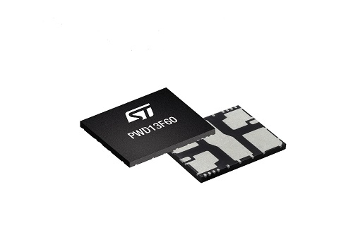
Fig. 1: STMicro’s SiP solution is targeted for industrial motor drives, lamp ballasts, power supplies, converters, and inverters.
The shutdown circuitry protects the power switches, and undervoltage lockout prevents malfunction with low voltage. Likewise, the bootstrap diode reduces the bill of materials (BOM) and simplifies board layout.
It shows how the choice of a package is crucial to maximize energy efficiency and accommodate a wide supply range. Here, it’s also worth mentioning that the power density of a package is intertwined with the improvements in thermal conditions.
3. Thermal efficiency
The thermal behavior of a package is intrinsically tied to its reliability because a component like an IGBT running at a lower temperature reduces stress on the component. Thermal characteristics also impact the heatsink size as lower temperatures translate into a smaller heatsink. Moreover, lower cooling requirements allow designers a higher margin for an increase in power density.
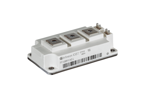
Fig. 2: Infineon’s power module package employs thermal interface material (TOM).
There are packages that retain the footprint and thermally efficient bottom-side design of the package while they expose the top-side source electrode as a venue for heat dissipation. That results in a higher current rating, which, in turn, leads to greater power density and smaller package footprints.
4. Heat dissipation
The conventional methods used to create isolation inside packages are often expensive and difficult to handle. Furthermore, they are largely inadequate in managing the heat dissipation from high-power-density components like IGBTs.
So Infineon has introduced a package technology that it calls Trenchstop Advanced Isolation. The German chipmaker claims that the Trenchstop packaging technology can replace fully insulated packages (FullPAKs) as well as standard isolation foils. Infineon is targeting the new package at applications such as power factor correction (PFC) for air conditioners, uninterruptible power supplies (UPS), and power converters.
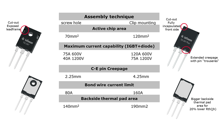
Fig. 3: The package on the right offers 15% less heat dissipation. Image source: Infineon Technologies.
Such isolation packages bypass the need for isolation materials and thermal grease, which allows designers to reduce the assembly time by up to 35%. At the same time, it improves reliability by eliminating misaligned foils. It also leads to improvements such as 10°C lower temperature than a FullPAK.
5. Switching losses
It’s imperative to minimize switching losses in order to boost the package efficiency, especially in hard-switching circuits operating up to 20 kHz in devices like industrial drives. Moreover, reliable switching and low EMI enhance heatsink-free operation in low-power applications.
Some packaging solutions feature an extra Kelvin emitter source pin to lower the switching losses (Fig. 4 ). It bypasses the emitter lead inductance on the gate control loop, enhancing a component’s switching speed and reducing the switching energy.
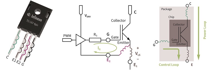
Fig. 4: A package with Kelvin emitter can reduce dynamic losses by up to 20%. Image source: Infineon Technologies.
Advertisement
Learn more about Electronic Products Magazine


