IEDM spotlights micro/nanoelectronic advances
An unusual item this year is a paper on electronic skin that gives a robotic arm a sense of touch. Researchers at the University of Tokyo (Tokyo, Japan) accomplished this feat by fabricating a large-area pressure-sensor matrix on a flexible plastic sheet�integrating high-quality organic transistors and rubbery pressure sensors.
Another topic generating growing excitement among many companies and researchers is strained silicon, a material that can make faster transistors that are compatible with CMOS fabrication processes. A research team from Taiwan Semiconductor (Hsin-Chu, Taiwan, R.O.C.) will describe 60-nm gate-length transistors made using silicon grown on a SiGe buffer layer tailored to get its lattice just right to strain the silicon.
A second team from Taiwan Semiconductor discusses the use of strain engineering to enhance a 65-nm silicon-on-insulator (SOI) process that incorporates multiple leading-edge elements. A paper from IBM (Hopewell Junction, NY) discusses the use of aggressive scaling and strain engineering to make high-performance logic devices with 45-nm-wide gates.
In the realm of memory, a research team from Infineon (Erlangen, Germany) has built a memory chip from an organic layer sandwiched between two sets of electrodes in a simple crosspoint array. When current is applied to the electrodes the organic layer changes states.
From the Tokyo Institute of Technology (Tokyo, Japan), a researcher will report on the possible use of ferroelectric material as a gate dielectric for a CMOS transistor. Such a device would be useful in a latch circuit with a temporary memory.
Another researcher at Cornell University (Ithaca, NY) will discuss recent progress in the development of memories based on the movement of just a few electrons. Underlying physics, technology tradeoffs, and compromises will be considered.
A process to create the smallest 40-Gbyte NAND-type flash memory cell ever will be described by Samsung Semiconductor (Kyoungki-do, Korea). The process uses 70-nm design rules.
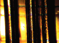
Other highlights from the conference will include several papers that describe the ongoing interest in using inexpensive organic material for making transistors and circuits. Researchers at the University of California (Berkeley, CA) will discuss how they built pentacene transistors directly on fibers. The transistors were fabricated without conventional lithography; instead, patterning was done via shadowing from overwoven fibers (see Fig. 1 ). The process is said to be compatible with textile manufacturing.

Fig. 1. Researchers at the University of California, Berkeley have formed arrays of transistors using weave-based masking.
In other developments, a team from Infineon Technologies will describe a thin-film transistor with an ultrathin self-assembling molecular monolayer gate dielectric and a pentacene channel. The resulting devices will operate at 2 V. Another team from Seoul National University (Seoul, Korea) will describe how it made silicon TFTs on plastic at acceptable 150°C processing temperatures, using excimer laser annealing and a special inductivity coupled plasma vapor deposition process.
Toshiba (Kanagawa, Japan) will describe a study of charge-carrier transport mechanisms in ultrathin single- and double-gated SOI transistors. The company fabricated devices with a 0.7-nm channel length, the equivalent of three silicon atoms wide.
Some papers will address issues at the frontiers of electronics. For example, a professor at Harvard University (Cambridge, MA) will review a general framework for the growth of single-crystal nanowires and will discuss their electrical transport properties and heterostuctures. Dr. Charles Lieber will describe nanotechnology-enabled applications like ultrasensitive chemical and biological sensors, along with the fundamental optical and optoelectronic properties of compound semiconductor nanowires and nanowire heterostructures.
Another researcher at the University of California (Santa Barbara, CA) will describe recent experiments that investigate the electronic, photonic, and magnetic manipulation of electron and nuclear spins in a variety of semiconductor structures. The paper will focus on the underlying physics for quantum information processing in the solid state.
�Christina Nickolas
*The International Electron Devices Meeting will take place December 8 to 10, 2003 at the Hilton Washington and Towers. For registration and other information, visit http://www.ieee.org/conference/iedm.
Advertisement


