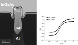
Imec, headquartered in Leuven, Belgium, has successfully demonstrated the first III-V compound semiconductor FinFET devices integrated epitaxially on 300 mm silicon wafers, through a unique silicon fin replacement process. The breakthrough enables future CMOS scaling down to 7 nm and below and enables new heterogeneous system opportunities in hybrid CMOS-RF and CMOS-optoelectronics.
At the core of new smart mobile devices will be advanced process technologies that allow for more power-efficient CMOS transistors and increased integration. Aaron Thean, director of the Logic R&D at imec commented that “During the last decade, transistor scaling has been marked by several leaps in process technologies…… The ability to combine scaled non-silicon and silicon devices might be the next dramatic transistor face-lift, breaking almost 50 years of all-silicon reign over digital ICs.”
Imec's process selectively replaces silicon fins with indium gallium arsenide (InGaAs) and indium phospide (InP), accommodating close to 8% of atomic lattice mismatch. The new technique is based on aspect-ratio trapping of crystal defects, trench structure, and epitaxial process innovations. The resulting III-V integrated on silicon FinFET device shows an excellent performance.

Imec's research is performed as part its core CMOS program, in cooperation with key partners including Intel, Samsung, TSMC, Globalfoundries, Micron, SK Hynix, Toshiba, Panasonic, Sony, Qualcomm, Altera, Fujitsu, nVidia, and Xilinx.
Advertisement
Learn more about Imec


