FPGA development tools available now eliminate many common bottlenecks
BY MICHAEL PARKER
Altera, San Jose, CA
http://www.altera.com
DSP-based processing is crucial to many of today’s consumer, industrial control, and medical systems. Building DSP-based systems using FPGAs can be challenging, and schedule delays happen all too often. Unexpected delays occur in design, integration, verification, feature requirement changes, and transition to production. However, FPGA development tools available now simplify the development cycle and eliminate many common bottlenecks.
Optimizing DSP performance
FPGAs provide the highest DSP performance available on a programmable platform, but optimizing a DSP algorithm in an FPGA can be difficult. Until recently, the algorithm needed to be ported to HDL and then the RTL functional simulation would be verified to match the high-level simulation test vectors.
Then the process of timing verification begins. The higher the required clock rate, the more pipelining and optimization is required. Timing closure can require multiple iterations and compilations. After timing closure, functional verification must be repeated.
If multiple channels must be processed simultaneously, the whole process is complicated further when the control logic and the memory must provide the proper time division multiplexing of the data flow, while maintaining the timing margins at the desired clock rate. If parameters such as channel count, FFT size, filter length, or system clock rates must be changed, then often the complete design must be updated and verified again.
However, this whole process can be automated, providing high-level design entry, simplified test-bench generation, variable channels, and optimized performance (at 400+ MHz). The process is controlled via parameters and changing the clock rate, increasing or decreasing the number of channels, or changing FPGA family involves just a few clicks and a recompile. This facilitates design reuse or late product specification changes.
Design teams often feel there is no time to adopt alternative design methodologies. There is a tradeoff between investment in better design and verification methods, and reductions in product development delays. There is also often skepticism that a new design methodology can actually deliver its promised improvement.
The risk of adopting a new design methodology can be dramatically reduced if it is compatible with current design flows, and can be introduced incrementally. This can allow specific areas of a design to be implemented and verified using the new methodology, and integrated with the rest of the design build using traditional HDL methods.
Risk can be reduced by gradual and systematic adoption, which can be influenced by both the actual productivity advantages and the learning curve. The design team retains the freedom to adopt the new flow only where the benefits clearly outweigh the initial time needed.
Modern design tools
Tools providing a higher level of design abstraction and productivity and delivering the performance of traditional optimized HDL are now available. One such tool is the new Simulink-based package called DSP Builder Advanced Blockset. This methodology uses a high-level behavioral description of the DSP algorithm.The design can be both simulated and instantiated into FPGA hardware.
A popular tool for block diagram circuit description is Mathworks Simulink. Within Simulink it is simple to create a diagram using elements such as registers, multipliers, and adders, in a intuitive and graphical form. A simple example, shown in Fig. 1, is the ubiquitous FIR filter the workhorse of DSP.
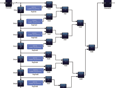
Fig. 1. A single-rate FIR filter described in Simulink.
Another very common construct in DSP systems is the fast Fourier transform (FFT). Advanced Blockset makes it easy to construct a textbook-like FFT implementation using a library of common primitive blocks such as butterflies and twiddle factors shown in Fig. 2 .
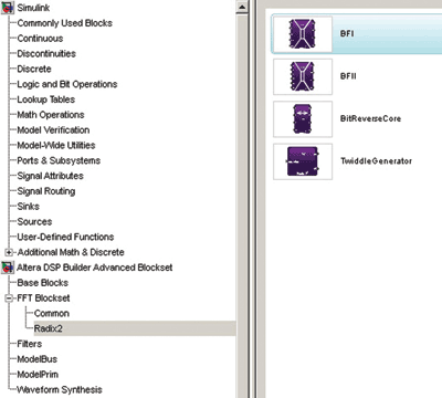
Fig. 2. An example of FFT building blocks.
The Simulink environment makes it is easy to add virtual sources, such as sinusoidal signals, modulated sources, or even noiselike signals, greatly simplifying production of test benches. Output signals can be terminated with virtual oscilloscopes and spectrum analyzers to view both time and frequency-domain responses and FFT or FIR filter response can be easily seen.
The test bench circuits can be implemented using any Simulink block, as The Advanced Blockset tool is also integrated with ModelSim, allowing easy comparison between the outputs of the Simulink design to that of the generated RTL using ModelSim. This ensures that the RTL produces a bit-exact match to the high-level Simulink output.
Many, if not most, DSP datapaths are multiple channel. The most common requirement is parallel processing of I and Q quadrature signals. In order to make this a multichannel design, simply add “ChannelIn” and “ChannelOut” blocks to the design diagram. There is no need to design logic to time-division-multiplex the DSP circuits among multiple channels, this is done automatically.
Simulating the design
The simulation within Simulink will activate the Advanced Blockset tool in the background each time it is run, and what’s happening in the background is what’s interesting. The Advanced Blockset tool takes the Simulink behavior model, along with parameters provided and performs a timing driven synthesis of RTL, using the built-in timing models for each FPGA and speed grade built into Quartus II design software.
The Advanced Blockset tool will add pipeline registers and control logic as necessary to achieve the clock rate provided. Also, by adding the channelization blocks from the Advanced Blockset library, the tool automatically configures the FPGA registers and control logic to perform time division multiplexing, so the high-clock-rate filter can process multiple lower-speed channels. In all cases, the Advanced Blockset tool will use multiplier and logic resources as necessary to provide the aggregate number of MMAC per second to perform DSP processing over the specified number of channels using the specified clock rate contained in the parameter file.
This is all done automatically and the results reported to the TimeQuest timing analyzer in the Quartus development software. In many cases, the performance level will be limited by the FPGA-hardened multiplier Fmax . This is common for filter designs with 100+ taps and 16 or more channels.
The question of latency
Latency is not inherently deterministic, as the Advanced Blockset will need to adjust this in order to accommodate the requested clock rates and channel counts. However, tool features are available to manage or constrain latency on a design block subset basis, allowing perform-design exploration and tradeoffs with unconstrained latency.
Once a design configuration and performance level is selected, the latency can be constrained to allow for predictable interfacing to the remainder of the surrounding implementation. If excess latency is selected for future design flexibility, the tool can add output register stages to match.This allows building a design once and easily updating to add channels, change system clock rate, and port to other FPGA devices as needed.
The Advanced Blockset is not limited to simple FIR filters. Reference designs and IP blocks are provided in the tool to allow rapid and highly optimized design of interpolating and decimating FIR filter, CIC filters, IIR filters, radix 2 FFTs, non-radix two FFTs, and many other DSP functions. It can also be used to build complex subsystems, such as a multichannel FFTs, digital up or downconversion chains, or crest factor reduction algorithms, for example. ■
For more on FPGAs, visit http://www2.electronicproducts.com/DigitalICs.aspx.
Advertisement
Learn more about Altera


