Core speed is only the start; wait states and code efficiency can be equally important
BY STEVAN DOBRASEVIC
Renesas Electronics America
San Clara, CA
http://am.renesas.com
With MCU performance and peripherals largely determining the overall capabilities of an embedded design it is easy to see why preoccupation with a popular core drives many MCU-based projects. But when you design a system with a given MCU not only do you want a core that delivers superior DMIPs/MHz performance, you must consider the different approaches taken to implement on-chip memory, the bus infrastructure and efficiency of multiple buses, code efficiency, and the core’s ability to service peripherals. You need to look at the entire MCU subsystem. To elucidate, we’ll use some real-world solutions found by the Renesas Electronics design team in developing its 32-bit RX MCU, which blends RISC and CISC architectures, while adding DSP and floating-point math.
The core of the matter
At the heart of every microcontroller is the CPU the processor core. In discussing core performance vendors usually rely on the Dhrystone program, which is representative of general performance and provides a DMIPS/MHz benchmark.
For current 32-bit midrange cores typical Dhrystone scores range from less than 1 to about 1.5 DMIPS/MHz. The RX core achieves 1.65 DMIPS/MHz when running at 100 MHz directly from flash with no cache or memory accelerator.
Overall core performance is a function of the number of instructions and the cycles/instruction. For many years, two different approaches have been used to obtain performance gains.
Traditional CISC (complex instruction set computing) instruction sets included many instructions of varying lengths. CISC instructions would typically enable operation directly on memory and support many types of addressing modes. The downside, however, is that many instructions take multiple cycles to execute, making them difficult to pipeline; also, with longer instruction lengths comes longer interrupt latency.
On the other hand, RISC (reduced instruction set computing) architectures obtained performance gains by creating fast instructions focused on reducing the number of cycles/instruction. To achieve single-cycle instructions, RISC processors use a fixed instruction length and only allow load and store instructions to operate on memory. Shorter, simpler instructions resulted in faster interrupt responses. The major disadvantage of RISC architectures is that due to their load/store nature they require larger code sizes.
Taken together, and based on the tradeoffs just discussed, if you were tasked with designing a more effective, efficient MCU, you might want to draw on the best elements of both worlds, creating a core that is a blend of CISC and RISC techniques an approach used by the RX processor.
Eliminate wait states
Of course, a fast CPU serves no purpose if the memory subsystem lags behind the processor. In a perfect world, memory should be able to supply instructions and data to the processor as fast as the CPU needs them without wait states injected into the execution flow. Many applications use flash as the primary code-storage memory, but flash memory read cycles are not always sufficiently fast for zero-wait-state access – especially given the escalating clock rates of MCUs. Some suppliers have turned to what they call a memory accelerator (read: cache) for flash. However, cache hit rates can be imperfect and MCUs will still suffer through wait states.
It is important to note that to run the MCU at a frequency above the native flash speed, wait states must be used and these degrade system performance. For example, consider a microcontroller core with a theoretical maximum of 1.25 DMIPS/MHz used with 30-MHz flash.
When running up to 30 MHz, no wait states are required and the instruction fetch can occur in one cycle, achieving 1.25 DMIPS/MHz. However, above 30 MHz, a wait state must be inserted as the instruction fetch now takes two cycles waiting for the memory access; therefore, it’s no longer possible to achieve 1.25 DMIPS/MHz. Memory acceleration techniques such as 64- or 128-bit-wide flash, instruction prefetch queues, and branch caching help, but embedded control applications have many branches, making it impossible to completely eliminate the hit to performance.
Registers and code efficiency
Using registers instead of memory to store values makes the process faster and cleaner. The number of registers available on a processor and the operations that can be performed using those registers has a significant impact on code efficiency. The problem with many processor cores is that there are too few registers (often 8) so performance drops and code size increases due to frequent save/restore processing in the register. While increasing the number of registers shrinks code size and improves performance, too many boosts chip size and complexity.
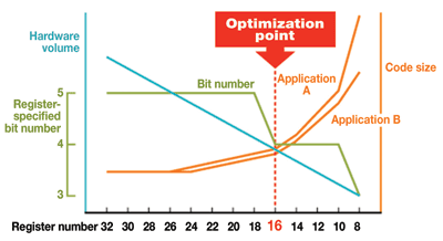
In developing the RX series, engineers examined customer code, looking into the effect of register number on speed, code, and chip size. The study found that a configuration of sixteen 32-bit registers is the best result in this tradeoff (see Fig. 1 ).

Fig. 1. Analysis of register optimization.
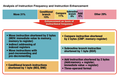
The RX development team also determined the most frequently used instructions. Move instructions comprise 31% of the code in a typical application and received the most enhancements in terms of additional addressing modes, and the ability to automatically increment and decrement values stored in registers.

Fig. 2. Analysis of instruction frequency and enhancement.
Conditional branch instructions were the next most frequent (15%) so the design team shortened the op codes for some branch instructions. The team also found a way to trim compare instructions. The net result of these improvements was a 28% code-size reduction.
Interrupt latency
Embedded designs usually require fast response to interrupts. Interrupts put on hold the normal program flow, execute an ISR, and then resume normal program flow. During an interrupt the intermediate results (registers) must be saved before the ISR can run and restored when the ISR is finished. The goal is to minimize the time between the interrupt by a device and the servicing of said device, translating directly into better system performance.
Normal interrupts such as found in most 32-bit cores store the relevant registers on stack by using push/pop instructions, which can result in multiple cycles of latency. The RX design supports normal interrupt handler implementations and also can be configured with a Fast Interrupt Function. This function uses three additional control registers. The registers are the BPC (backup PC), BPSW (backup PSW), and the FINTV (fast interrupt vector register). When the designated fast interrupt occurs, the MCU can store the PC and PSW to the backup registers and read the interrupt vector from the FINTV register. The programmer can also chose to configure four general-purpose registers for dedicated interrupt processing, eliminating the need to save register state to memory before entering an ISR and further speeding response time. That’s not a realistic option on most MCUs that have only eight general-purpose registers, but is viable when you have 16 registers.
A blend of CISC and RISC
Using primarily a CISC architecture, but with a hybrid approach, a processor family can deliver significant code density advantages over RISC designs and overcomes traditional CISC downsides by using 16 general-purpose registers and implementing a five-stage pipeline and out-of-order instruction completion, which results in mostly single cycle instructions. ■
Advertisement
Learn more about Renesas Electronics America


