Integration vs stand-alone PMICs: Systems need both
All-in-one PM architectures save board space, cost but may not be able to address design needs without compromising systems
BY GEORGE PAPARRIZOS
Marketing Director
Summit Microelectronics
www.summitmicro.com
The smartphone and tablet market segments are two of the fastest growing ones in the electronics industry. Today’s typical system designs are very different from the ones of just a couple years ago. The adoption of multi-core, high-performance processors, combined with the use of high-resolution displays and high data-rate wireless connectivity have significantly changed the power requirements in new designs. At the same time, new Li-Ion batteries with increased capacities and higher voltages are used to maintain acceptable run times. These design trends are posing new challenges to the power management chips and will re-define the power architecture in modern portable devices. While multi-channel power management ICs have traditionally benefited portable applications in terms of cost and space savings, in many designs the high-level of integration is becoming a limiting factor for high-performance operation and demanding industrial designs.
Mobile system trends and challenges
While larger batteries are providing higher capacity and in theory more talk/standby time in smartphones, the use of power-hungry components finds place at a faster rate than both battery technology improvements (higher energy density) and capacity increases. As such, run times remain unsatisfactory to the majority of users. At the same time the usage model for both consumers and professionals is dramatically changing; users are utilizing their mobile devices and are connected all the time, in many places and are highly dependent on them for everyday activities. Given these trends, fast-charging from any battery state (level), especially when system is running, is becoming very critical.
The tablet market is still in its early growth stages and as such it is much more fragmented than the smartphone market. Today’s offerings include display sizes as small as 5 in. and as large as 13 in. The display size and consequently the industrial design have a large effect on the battery pack used, with the main goal of maximizing usable battery life without significantly increasing the tablet’s s-dimension (thickness). While the majority of today’s designs use multiple battery cells in parallel, as the display size increases so do the benefits of a serial battery cell approach, especially in terms of total system efficiency.
New system designs can vary significantly from each other and these differences are driven by many factors: cost, space, performance, flexibility and industrial design. As such power management requirements can be very versatile and the traditional one-solution-fits-all approach does not meet expectations. On a very high level, the decision between one or two source inputs and one or two (CurrentPath) outputs has a large impact on solution size and cost. Furthermore, applications differ significantly in terms of battery capacity and thereby in terms of required charge current levels. Other considerations include support of specific industry specifications, use of a wide variety of power sources (USB, ac/dc, wireless, high-voltage), level of system control, adoption of new battery technologies and others.
High-integration solutions
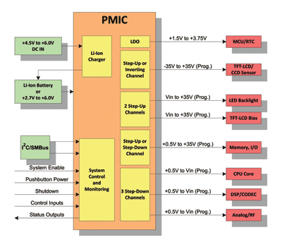
Highly-integrated power management chips are commonly used in conjunction with specific application processor and baseband chips with the goal to address the vast majority of their power management needs. Since these power management integrated circuits (PMICs) are developed around a specific platform, they “understand” most of the system requirements very well. A typical application is shown below in Fig. 1 . The absorption of most required functions on a single chip has many advantages, with the most important one being the reduction in component count and consequently in solution space. High integration may also guarantee a more reliable and effective interaction and co-operation among the different power management blocks since they can be defined in a very controlled fashion. Examples of such synergies include power-on sequencing, power delivery prioritization, and system monitoring.

Fig. 1: Typical PMIC solution
Standalone charging solutions
While the adoption of high channel-count power management ICs is benefiting many applications in terms of space and cost, some of the latest mobile design trends have introduced severe limitations in the system. The charging circuit for example, needs to be located close to the power input, that is, the connector of the mobile device. On the other hand, the main dc/dc regulators benefit by being located close to the CPU. This conflict makes the board layout and the corresponding IC location very challenging. Furthermore, the charging IC being the main component that connects the outside world to the phone, requires extra safety features to protect itself and the downstream system. As such, many charger ICs need to tolerate high input voltage levels in case of a non-qualified or faulty external power source. In the case of a high-integration PMIC, adding this high-voltage tolerance may penalize the entire chip in terms of size and consequently cost.
The thermal behavior of the mobile device also has a large impact on system performance and adds critical barriers on the charging functionality. As the processor chips become more power hungry and require higher levels of current, the power dissipation of the PMIC becomes very high and to maintain reliable operation, some of the peripheral power functions on the PMIC are being suspended or reduced. In a typical system design the dc/dc regulators for the main components (core, I/O, memory) need to remain active for the system to keep running to guarantee good user experience. During high temperature rises, the battery charger current is however reduced to allow for the PMIC temperature to fall within acceptable limits. Making things worse, as temperature rises, so do the resistances of the power FETs, which further accelerates power dissipation within the device.
High temperature rises on a highly-integrated PMIC also generate vary localized hot spots, making in many cases the thermal problem a very serious issue. As many of the new portable devices focus on industrial and compact design, this heat generation becomes a show stopper for many projects. Separating charging functionality from the main PMICs reduces localized hot spots and enables a more thermally forgiving design. Figure 2 shows an example of temperature rise for an integrated and a dis-integrated solution for two functions generating the same level of power.

Fig. 2: Example of power dissipation
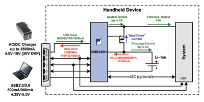
Another design challenge in highly-compact modern electronic devices is the isolation of electric noise from RF circuits. Such noise can result to electro-magnetic Interference and affect the performance of the tablet or smartphone. The integration of a switching battery charger on a PMIC introduces another source of noise (see Fig. 3 ), which can easily be coupled into other PMIC dc/dc channels and negatively impact many RF-sensitive components.

Fig. 3: Typical standalone charging solution
The increasing complexity and power requirements of new portable devices combined with an ever changing usage model is introducing new system design challenges. Traditional and all-in-one power management architectures are very advantageous in terms of board space and component cost. However, such solutions may not be able to address all the modern design needs without compromising important system attributes. Enabling safe, reliable, fast and universal charging requires the use of the optimum charging solution for a specific application. As such, dis-integration in many cases is becoming a better approach and can benefit the system in many different ways.
■
Advertisement
Learn more about Summit Microelectronics


