Interconnects: Transitioning from micro to nano
Shrinking cables have different needs as they move inside the box
BY BOB STANTON
Omnetics Connector, Minneapolis, MN
http://www.omnetics.com
BILL LEE
LEMO USA, Rohnert Park, CA
http://www.lemo.com
Today’s electronic systems have changed significantly as a result of the increased capability of the silicon chip industry. System capabilities, functions, and processing are increasing at dynamic rates.
Increased functionality of today’s systems is requiring cables to keep pace.
Good system design continues to demand high-reliability cable systems, often with increased wire counts, routed into the main instrument panel. Inside the instrument, signals, data processing, and probe cues must be routed to a wide range of ever-smaller modules focused on processing their selected functions.
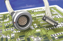
As module functionality increases, so does the density inside, and modules are reduced in size to nearly micro-sections. Micro-connectors at 1.3-mm spacing and nano-connectors at 0.625-mm spacing can significantly reduce size and weight of interconnects in newer systems.
Where are the connections?
As density increases and modularization continues, the design engineer’s task is to provide two different interconnection levels to accommodate the larger instrument with panel requirements and the internal systems. The first connection is from the system probe that provides data acquisition or provides a service or process, such as a laser, optical camera chip, or rotating tool. The second connection is a compact system inside the box that extends the cable routing to a multitude of miniature modules and printed wiring boards.
Into the box
Macro-to-nano transition cables address this very issue. Connector and cable systems routed from outside services into the instrument’s front panel face demanding challenges. The probe, or service end of the cable system, is often customized to fit the ever-changing applications that sometimes even include the recent movement of active-chip technology out at the end of the cable itself.
Typically, the cable must be rugged, flexible, and shielded, and yet feel good personally to the user. The connector must both survive the rigors of being whipped about the end of the cable and smoothly plug into the mating panel connector without problem.
It also must continuously mate over thousands of cycles and maintain both its polarity and visual quality. Often, the quality of a good cable system is tested at the cable-to-connector interface.
This transition point is critical to maintaining a good jacket seal or EMI protection for the rest of the system. Connector design support is often needed to ensure the designer meets and exceeds the challenges of getting a good signal into the instrument or driving a unique instrument out at the end of a cable.
Experienced manufacturers offer a wide variety of options based on the highest reliability and performance levels. Suppliers can sort through the various product demands and match up a best offer or analysis that would yield a cable connector system to serve the instrument including the panel-mounted connector to route signal systems inside the box for distribution inside the instrument.
Inside the box
The environment changes dramatically inside the instrument. Temperature conditions, personal handling, shock, and vibration issues must be addressed differently.
The unique challenges inside the box can be as difficult to address as those outside. Electrical noise is more concentrated and sensitive inside the box, and as the amount of chip processing escalates, issues of signal speed, crosstalk, and EMI coupling can hinder design successes quickly.
Additional challenges include routing signals in and around boards and modules in multiple directions and elevations while trying to keep wire length as short as possible. (Another point to remember is that the best impedance match includes short interconnection lengths.)
Although additional functions can add weight to the instruments, which is unattractive to the user, advances in chip technology bring decreasing voltages and current-flow levels. This paves the way for use of micro- and nano-sized connectors with smaller, more flexible wiring between systems. The new nano-connector systems pass even the highest quality and reliability testing demanded and can be trusted to meet instrument-level requirements.
The advantage is more room and weight for other electronics inside the box. Most nano-connectors provide high-density SMT formats to fit onto the smallest of circuit boards used in the instrument equipment. ■
Advertisement
Learn more about Omnetics Connector


