Silicon carbide (SiC) power devices have been commercially available for ten years. During that time, there has been a steady increase in voltage ratings to 1,200 V and 1,700 V for SiC-Schottky diodes, and more recently, SiC-MOSFETs with device current capability >50 A in a single die. With these increased voltage and current ratings, it is now possible to implement standard hard-switched power inverter designs that replace conventional silicon devices with all-SiC power components, creating smaller, lighter, more efficient power inverters to several hundred kilowatts that operate at significantly higher switching frequencies with superior thermal characteristics.
This new generation of power inverters can be implemented for alternative energy sources such as solar and fuel-cell inverters, industrial motor drives, uninterruptible power supplies, three-phase industrial power supplies and soon, large traction and wind applications.
Comparing SiC MOSFET vs. Si IGBT
The first consideration in inverter design is sizing components to meet system voltage and power requirements. Maximum current ratings and device conduction losses set the initial inverter module current ratings. Due to inherent low switching loss, an all-SiC inverter design, (usually implemented in power modules), requires less rated amperage to support a given design. For example, Cree’s 1200 V/100 A SiC-module exhibits significantly lower average conduction losses than a competitive 1200-V/150-A Si-IGBT module across the inverter’s normal operating range, (Fig. 1 ). In conduction mode, the unipolar SiC MOSFET acts like a resistor. In contrast, a bipolar IGBT device behaves like a resistor in series with a diode. Figure 2 illustrates similar conduction losses for 100-A SiC-MOSFET and 150-A IGBT modules at 25°C and 150°C. However, as the load current is reduced, IGBT voltage remains relatively constant and SiC-MOSFET voltage reduces linearly based upon its RDSon. Referencing the IV chart, at 50-A load, the SiC-module dissipates 50-W losses, while the IGBT dissipates 65 W, for a 23% improvement in conduction losses. The result is significant reduction in conduction losses over the average inverter operation. Silicon IGBT-based systems typically over-rate the current capability of modules to achieve acceptable efficiency ratings. SiC-based inverters require much less derating.

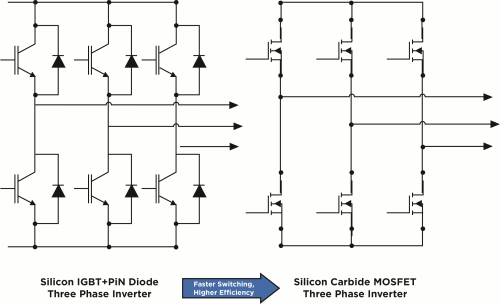
Fig. 1. Three-phase inverter designs implemented in silicon IGBTs (left) and SiC MOSFETs (right)

Fig. 2. Total conduction loss comparison (switches & diodes) for 1,200 V/100 A SiC MOSFET module vs. 1,200-V/150-A Si IGBT module operating at 25°C and 150°C
Switching loss comparison
Comparative advantages of SiC vs IGBTs are even more pronounced in switching losses. Because of superior switching performance in SiC devices, a 1,200-V/100-A SiC MOSFET module can replace a 1,200-V/150-A Si-IGBT module in a typical dc/ac three-phase voltage source inverter (VSI) design even at a relatively low switching frequency (5 kHz). As switching frequency goes up, this current rating advantage grows significantly. In a typical VSI rated for 415-Vrms/75-Arms output, the two devices were simulated at frequencies of 5 kHz and 16 kHz. As shown in Fig. 3 , total switching loss comparison between modules at 5 kHz reveals SiC-MOSFET module losses that are 4x to 7x lower than the comparably-rated Si-IGBT module.

Fig. 3 : Total switching loss comparison (switches & diodes) for 1,200-V/100-A SiC-MOSFET module vs. 1,200-V/150-A Si-IGBT module operating at 25°C and 150°C
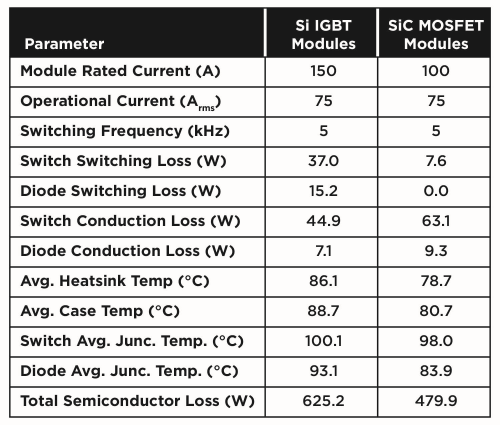
Improved switching performance enables higher system power or higher thermal margin, resulting in a trade-off between lower cost-per-kW and enhanced system reliability. Thermal performance enhancements can be further seen in the simulation results (Table 1 ). At the VSI’s full rated load of 75 A and 5-kHz operating frequency, with equal heatsinks, SiC-MOSFET module losses are 13.7% lower than the Si-IGBT module. Overall semiconductor device losses are reduced by 23.2%, or 145.3 W. In addition, heatsink and case temperatures are reduced by 7.4°C and 8.0°C.

Table 1: VSI simulation parameter comparison between 1,200-V/100-A SiC-MOSFET module and 1,200-V/150-A Si-IGBT module at 75-A maximum load, 5-kHz switching frequency
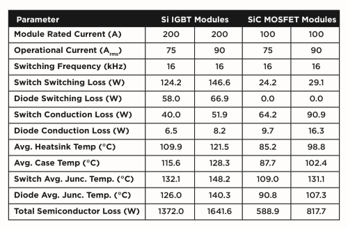
Increasing the VSI switching frequency to 16 kHz reveals even more pronounced benefits of the 1,200-V/100-A SiC-MOSFET module’s superior switching and thermal performance. At the nominal 75-A maximum output, an increase to 16 kHz requires replacing the 1,200-V/150-A Si-IGBT module with a 1,200-V/200-A Si-IGBT module; but even increasing the amperage to 200 A, there is insufficient thermal margin to ensure reliable operation. Employing a Si IGBT module at this frequency with adequate thermal margin requires an increase to 250A or 300A. As shown in Table 2 , at 16kHz the 100-A SiC-MOSFET module exhibits total semiconductor switching losses that are 57.1%, or 783.1 W, lower than the 200-A Si-IGBT module, translating to significantly lower heatsink, case and junction temperatures and a corresponding increase in operating reliability. Increased switching frequency enables the inverter to operate outside of humans’ audible range, providing ergonomic advantages; or, by significantly reducing the size, weight and cost of the inverter’s filter inductors and capacitors, providing an economic advantage.

Table 2: VSI simulation parameter comparison between 1200V/100A SiC MOSFET module and 1200V/150A Si IGBT module at 75A maximum load and at 90A overload, 5kHz switching frequency
The best of both worlds
Beyond the VSI simulation results, comprehensive analysis of SiC MOSFET modules and Si IGBT modules in a real-world 250-kW inverter applications shows the SiC-MOSFETs deliver superior switching performance with significantly lower switching and conduction losses, reduced thermal characteristics, and improved efficiency.
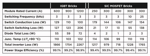
A 300-A all-SiC module operating at 10 kHz has significantly lower losses than a 900-A Si-IGBT module operating at 3 kHz (55-W vs. 123-W losses in the switching devices, and 2-W vs. 59-W losses in the diodes – see Table 3 ).

Table 3: Comprehensive analysis of losses in a 250kW inverter between SiC MOSFET modules and Si IGBT modules
Cost/performance considerations
As illustrated above, SiC technology enables inverter designs with improved efficiency using SiC components that are significantly smaller than Si IGBTs. Benefits of SiC switching losses are well-documented and understood; however, further improvements in system efficiency for conduction losses extend SiC benefits to lower system switching frequencies. SiC provides the system designer flexibility to optimize efficiency and increase switching frequency to minimize system size, weight and cost. These benefits result in lower overall power component cost, provided the designer takes full advantage of SiC switching and conduction advantages and correctly specifies the SiC components required to meet power and efficiency targets.
Driver considerations for SiC-based inverter designs
Once SiC MOSFET and Schottky diode devices are sized appropriately for the system, several device attributes must be considered for overall SiC design; most importantly, optimizing SiC MOSFET drivers. Early SiC MOSFETs exhibit lower transconductance than mature silicon MOSFETs, (this issue is being mitigated), as it was in early-generation silicon devices. SiC gate drivers need to provide minimal gate charge, but a large voltage swing to ensure minimum switching losses. SiC MOSFET makers highly recommend gate drive voltages from 0 to 20 V. A small negative gate voltage provides additional system noise margin and contributes to more switching efficiency. Further advantage can be gained by driving gates with a high dV/dt. Best efficiency results from transition times
SiC-based power modules advantages
As mentioned above, power devices in most inverter designs higher than a few kilowatts are implemented in power modules. These modules can implement single switches, half-bridges, full bridges or three-phase integrated inverters. A growing list of vendors have implemented all-SiC versions in custom and standard configurations. As these modules are relatively new, designers can expect a rapid expansion of available choices, including one from Cree – a 100-A, 1,200-V half-bridge module; fully released and available from major distributors. Optimized for lowest inductance and incorporating gate resistors in close proximity to the SiC MOSFET gates, the module features an AlSiC baseplate with Si3N2 insulator to ensure excellent thermal performance and rugged reliability in a lightweight housing. Combined with driver boards available from Cree, this type of module represents the potential system design advantages possible with SiC.
Advertisement
Learn more about Cree


