Lab-on-chips will revolutionize healthcare. And, silicon will revolutionize lab-on-chips. The technology that made ICs into the greatest success story ever, will now be used to put diagnostic tests in the palm of your hand.

Figure 1: This picture shows the future in which we will use compact diagnostic tools to do very fast blood tests.
What are lab-on-chips?
A lab-on-chip is a device in which a sample (e.g. blood) moves through miniature channels to integrated mixers, reaction chambers, detectors etc. All these components have one common goal: to detect a target in the sample. This can be proteins, metabolites, ions, or even DNA and RNA.
LOC devices will enable for doctors and patients to do fast diagnostic tests. In a first phase, lab-on-chip systems will be available at the doctor’s office or in the hospital (point of care) as desktop tools in which a cartridge with a blood droplet has to be inserted. The cartridge is disposable and houses the microfluidics and sensors. In the desktop tool, external pumps and heating elements move the fluids in the cartridge and allow the chemical reactions to run at the right temperature.
But eventually, it will be possible to shrink this whole system, including pumps and heating elements, into a few cm³ (see figure 1). And according to imec, the secret lies in the use of silicon as base material, even for the microfluidics part of the lab-on-chip.
Polymers or silicon?
Different materials (polymers, glass, and silicon, and combinations of these) can be used to make the miniaturized structures that make up a lab-on-chip system. Surely, the most widespread option today is polymer. Silicon is considered as a too expensive option. However, this is only the case when you would make a simple passive microfluidic chip with just a few simple components, like microchannels and a mixer.
The strength of silicon only surfaces when you make lab-on-chips with a myriad of very fine channels, reactions chambers and sensors. When integration and sensing are the key assets of the system, then silicon is definitely the best option. Parallelization is another huge plus of using silicon. The silicon technology is extremely good at making hundreds of structures in a cost-effective way. So, for lab-on-chip applications in which compactness, ultrafine, and large amounts of structures are important, silicon is the winner.
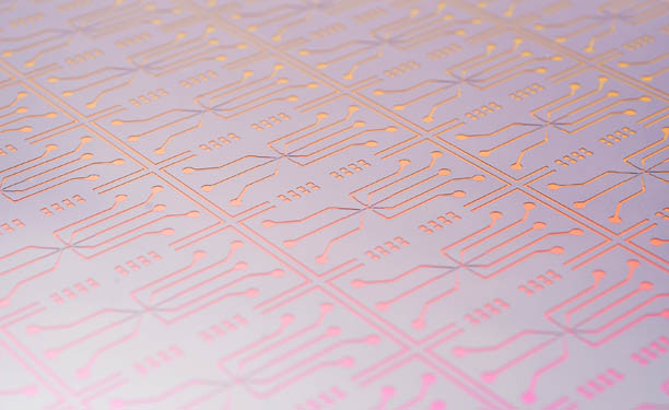
Figure 2: Lab-on-chip structures made on a silicon wafer.
First, a silicon wafer is patterned using e.g. lithography and dry etch (figure 2). When complete, the structures are sealed with glass. At the back of the wafer, fluidic connections are carved out to be able to connect the system to the reagent reservoirs and outlets.
A silicon-based platform for microfluidics
To prove the potential of silicon for microfluidics, imec (Leuven, Belgium) has developed a process flow building on its semiconductor fabrication expertise. Both coarse (500 – 3 µm) and fine (3 – 0,5 µm) structures can be made within the same flow, which is not obvious when using deep silicon etch techniques. This gives large design flexibility. Also, structures with high aspect ratios can be fabricated (up to aspect ratio 40). A nice example of this are the high, narrow micropillars that were made for use as filters.
Future work focuses on introducing a backside metal layer into the platform to make thin-film heaters and temperature sensors. This will eliminate the need for external cooling and heating systems. Another adaptation to the platform will be to work out a low-temperature bonding (preferably room-temperature) process, which can replace the current anodic bonding that is performed at 400°C. This will allow developers to functionalize the chip within one and the same process flow.
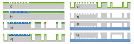
Figure 3: Fine and course structure process flow.
Figure 3 shows the process flow used to make both fine and coarse microfluidic structures on a silicon wafer. (a) A silicon wafer (grey) is covered with an oxide layer (green). The fine structures are patterned in the oxide layer that will be used as a mask for their fabrication in a later phase. (b) Then, a nitride layer (blue) is added. (c) An etch is performed to remove nitride and oxide and silicon is excavated to form the coarse structures. (d) The exposed silicon surface is oxidized. This oxide will serve as protection during the definition of fine structures. (e) The nitride is removed and the fine structures are etched, (f) the oxide is removed (g) the silicon is bonded to Pyrex. (h) Backside etch is performed to open fluidic connections. Note that, thanks to the fact that an oxide mask with nitride protection is used, it is not necessary to spin and pattern the resist for fine structure etching, which would be difficult due to the large topography of the already defined coarse structures.
Future work
As a first step towards silicon-based LOC systems, researchers have set up a silicon-based platform to make microfluidic structures. The process flow has been used to make a variety of structures: microchannels, mixers, microreactors, micropillar filters, capillary pumps and valves, droplet generators (for digital droplet PCR ), mergers, and splitters. The process has proved to be very stable and can be used for all sorts of designs.
Advertisement
Learn more about Imec


