Low-power direct digital synthesizer cores enable high level of integration
With advancements in performance and significant power savings, DDS components act as a powerful building block in frequency synthesis and timing solutions.
BY VALOREE YOUNG
Analog Devices
Norwood, MA
http://www.analog.com
A synthesizer based on direct digital synthesis (DDS) generates a sampled sine wave at a desired frequency and phase. While not nearly as ubiquitous as its analog cousin, the phase-locked loop (PLL), DDS is carving its way into more and more designs, thanks in part to improvements in spurious-free dynamic range (SFDR), phase noise, and power consumption.
Its inherent digital nature gives DDS technology definite advantages: extremely fast frequency switching, extremely fine frequency tuning resolution, precise phase adjustment, unparalleled quadrature phase matching, accurate frequency, phase, and amplitude modulation, and flexible digital programmability. Historically, direct digital synthesizers have served the military and high-end test and instrumentation markets almost exclusively, as these industries were less sensitive to the higher cost and power consumption traditionally associated with DDS.
Today, however, the need for smaller components with reduced power is becoming critical for a number of emerging applications, even within these industries. Reducing the core power of the DDS device not only helps lower overall system power consumption, but allows DDS core integration to be used in a variety of ways, including easy multichannel synchronization, targeted spur reduction, digital PLL timing, and agile modulation.
Understanding the basics
To fully appreciate the qualities and benefits of a direct digital synthesizer, it is important to first understand the basics of the technique. At the center of a DDS system is the phase accumulator — a modulus counter that increments a stored number on each cycle of the system clock.
The stored number resides in a delta phase register and is repetitively added to the running total at the output of the phase accumulator. Note that the accumulator is allowed to roll over. The result is that the output of the phase accumulator is a sawtooth waveform that represents the linearly changing phase of a sinusoid.
The output of the phase accumulator can thus be used as the address to a sine (or cosine) lookup table (some DDS designs have replaced the lookup table with algorithms). Since each address represents a phase value, the “lookup” value represents the amplitude of a sine or cosine function. With a linear ramp as the phase input to the lookup table, the output is a digital sine or cosine wave. This sinusoidal amplitude information is the input to a D/A converter (DAC).
Although the theory behind DDS architecture has changed little over time, the speed, resolution and capabilities of the technology have continued to progress. State-of-the-art DDS chips (processed on CMOS technology) clock at 1 Gsample/s, with outputs up to 400 MHz and integrated DAC resolutions up to 14 bits.
It is not accurate to focus solely on these specifications in defining modern DDS devices, however, as today’s increasingly complex systems demand multiple dimensions of performance. A secure radar system may rely on both high-frequency operation and frequency-sweeping capability, while communications equipment may require the best phase-noise performance at the lowest cost.
In an effort to accommodate widespread applications, available DDS products offer an elegant array of functions and performance enhancements that are well suited to many markets. Speed, DAC resolution, frequency- and phase-tuning resolution, phase noise, SFDR performance, integration, packaging, power, cost, and special features are just some of the parameters to consider when choosing a direct digital synthesizer.
Within the portable and handheld markets a need exists for high performance at low cost and low power. Not typically considered a contender in this arena, new low-cost DDS ICs — running at high speeds with very low power consumption — are now entering the playing field.
Operating at clock speeds up to 250 Msamples/s, these devices provide analog outputs to 100 MHz while consuming just 50 mW of power. The need for reduced power has expanded into many industries.
As technology continues to invade the battlefield, the trend is to outfit soldiers and vehicles with secure handheld communications, analyzers, detectors, and other portable equipment. A similar trend is taking hold in the medical field as portable diagnostic tools and home monitoring equipment become widespread.
Applications requiring multiple synchronized outputs, such as phased-array radar systems, optical communications, automatic test equipment, and medical imaging, can benefit greatly from a multichannel DDS implementation. Up to four independent, programmable synthesizers are synchronized to a common clock, enabling digital precision found nowhere else.
Until only recently, this concept was not reasonable due to the high power consumption of a single DDS core. Today however, available multichannel DDS devices can be clocked at 500 Msamples/s, producing analog outputs up to 200 MHz while consuming only 165 mW per channel. This is not a bare bones synthesizer either; the multichannel DDS performs 16-level frequency, phase, or amplitude modulation (FSK, PSK, ASK) and supports linear sweep capability. The simplicity of multiple DDS channels integrated on a single IC also saves designers time and effort as compared to the difficult task of synchronizing multiple components in a complex system design.
Integrating DDS
Analog Devices’ patented spur cancellation technology using destructive interference is a unique architecture that takes advantage of lower-power DDS cores. By creating an auxiliary signal generation path to replicate the primary signal, digital elimination of the harmonic spurious content typically introduced by the DAC is possible.
Programming the spur reduction channel to match the problematic spur’s frequency and amplitude, then adjusting it to be 180 degrees out of phase, reduces the magnitude of harmonic spurs in the synthesizer output spectrum. The implementation of multiple spur reduction channels is now an attractive architecture due to lower-power DDS cores.
The AD9912 from Analog Devices integrates two additional DDS cores that can be used to pinpoint and significantly reduce two different harmonic spurs. With the internal clock running at 1 Gsamples/s, this DDS produces analog output frequencies up to 400 MHz from a 14-bit DAC, while typically consuming only 700 mW. With a 48-bit frequency tuning word (FTW), frequency resolution of 3.6 μHz is possible, along with 0.022° of phase tuning resolution.
New DDS cores also boast exceptional phase noise performance due in part to improvements in the system clock input receiver design. Operating from a 1 GHz system clock, with the DDS in divide-by-8 (integer) mode, producing 125 MHz output, the residual phase noise floor is down at -165 dBc.
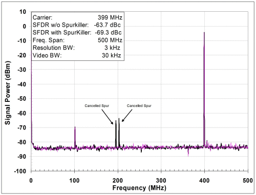
To observe the spur cancellation function in action, see Fig. 1 . The plot shows the synthesizer’s output spectrum for a 399 MHz sine wave, with a 1-GHz sampling rate. The purple line demonstrates improvements to wideband SFDR after performing the spur reduction technique, knocking the 2nd and 3rd harmonics down to the noise floor.

Fig 1. The plot shows the synthesizer’s output spectrum for a 399-MHz sine wave, with a 1 GHz sampling rate.
An advanced clocking architecture that benefits from the strengths of DDS technology is the digital PLL. Combining a digital phase detector with a direct digital synthesizer offers some enhanced features and flexibility as compared to an analog PLL approach.
Specifically, a DDS-enabled digital PLL may include a programmable digital loop filter capable of very narrow bandwidths (
The DCO removes the limitations associated with the tradeoff between VCO tuning range and phase noise. The signal purity of the output is instead dependent upon the DAC system clock, giving the designer more freedom in choosing a local oscillator source according to specific jitter requirements.
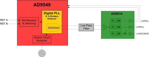
A complete clock synchronization, generation, jitter clean-up, and distribution circuit is shown in Fig. 2 , with the DDS at the heart of the system. This example places an ultra-low-jitter pin-programmable clock divider in the timing path, thus enabling programmable skew adjust.

Fig. 2. Shown is a complete clock synchronization, generation, jitter clean-up, and distribution circuit with the DDS at the heart of the system.
A DDS-based design is also a good candidate in agile digital modulation schemes, including base station transmit architectures, cable modems, and satellite communications. The DDS provides a near-perfect digital quadrature signal that can be used as a quadrature carrier signal.
With the addition of integrated digital I/Q baseband signal processing components, a completely digital quadrature modulator is possible. For example, a quadrature digital upconverter (QDUC) integrates a high-speed 1-Gsample/s DDS core, a high-performance 14-bit DAC, clock multiplier circuitry, digital filters and other DSP functions onto a single chip. A 250-MHz 18-bit-wide data input port supports interleaved data rates as high as 125 Msymbols/s.
All this is possible without excessive power consumption; in fact today’s QDUCs offer a decrease in power compared to previous generations while running at clock rates five times as fast. The QDUC supports real IF analog outputs up to 400 MHz.
With such dramatic reduction in power consumption, along with improved SFDR and phase noise performance, the DDS is beginning to expand beyond its previous duty as a simple frequency generation technique. Designers must understand the latest in DDS innovations, from minimizing cost, power, and size, to obtaining maximum speed, precision, and dynamic range so that they have access to all options when choosing a synthesizer-based solution. The old perception of DDS as a costly, power-hungry, standalone component has evolved, as its full potential as an integrated function has been recognized. A low-power DDS core combined with additional signal-processing blocks presents a powerful foundation for more complex systems.
For more on DDS products, visit http://electronicproducts-com-develop.go-vip.net/linear.asp.
Advertisement
Learn more about Analog Devices


