Low-voltage differential signaling:
Milliwatt power
at megabit speed
The technology offers inherent
advantages
in noise immunity and EMI
BY MICHAEL WILSON
National Semiconductor
Santa Clara, CA
Low-voltage differential signaling (LVDS) technology is poised to become the next great interface standard. LVDS, which defines the physical layer communication performed by line drivers and receivers, is being chosen over alternative technologies because of its advantages in speed, power, EMI, noise immunity, and cost.
There are two industry standards for LVDS: ANSI/TIA/EIA-644, approved in November 1995, and IEEE 1596.3, approved in March 1996. The former standard is the more generic and popular of the two, and is the basis of the discussion presented here.
The standard defines line-driver output characteristics and receiver input characteristics only, allowing referencing standards to determine the actual application specifics including protocol, connector pinout, and cable parameters (see Fig. 1 ). This flexibility allows LVDS line drivers and receivers to enjoy widespread use, ranging from notebook LCD displays and peripheral interconnects to datacom and telecom applications.
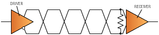
Fig. 1. The LVDS standard defines line-driver output characteristics
and receiver input characteristics for point-to-point connections.
Speed and power
The high-speed and low-power attributes of LVDS are unparalleled. The tradeoff between speed and power–a rule of thumb for older technologies–does not apply to LVDS.
With a recommended maximum data rate of 655 Mbits/s, LVDS greatly exceeds the speed of popular data-transmission standards like RS-485 and RS-422. And while PECL and ECL devices are capable of high data rates, they can consume up to 10 times more supply current than comparable LVDS devices.
LVDS power savings are not limited to just the power supply current. The drivers are commonly implemented as current-mode devices, which provide a flat ICC-versus-frequency characteristic. In addition, load current is minimized by a signal swing of 300 mV across a 100-ohm load, creating a loop current of only 3 mA.
Noise immunity and EMI
LVDS offers additional advantages because of its inherent immunity to noise and its low electromagnetic-interference characteristics. Any system noise that couples equally onto both differential transmission lines appears as a common-mode signal and is rejected by the receivers.
The standard specifies a common-mode voltage range of ±1 V with a 1.25-V offset. Although this range may not sound very large, it offers twice the noise margins of other reduced-swing interface standards such as BTL and GTL.
Reduced EMI is attributable to the low-voltage signaling (300 mV) and differential data-transmission scheme. TTL and CMOS signals are an order of magnitude larger and require a greater DV, thus generating more EMI than LVDS. PECL also has a larger voltage swing and higher EMI.Figure 2 compares the voltage levels of different signaling technologies.
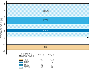
Fig. 2. Compared to other technologies, LVDS operates at lower voltage
levels and with a smaller voltage swing, resulting in reduced EMI.
In differential signaling, the majority of the current sourced by the driver is returned within the pair and not via the power or ground planes. The resulting EMI is very low, because fields generated by the pair cancel each other, and also because the ring antenna (created by the signal pair and termination resistor) is small.
Wide range of applications
LVDS can be used to great advantage in many different applications since the standard does not define the mechanical or functional specifications. The LVDS specifications are written for point-to-point configurations, but multidrop and multipoint applications can also be accomplished.
Point-to-point is uncomplicated, offers the best-case signaling environment, and is the easiest to implement. In multidrop (single-driver-to-multiple-receiver) and multipoint (multiple-driver-to-multiple-receiver) configurations, the propagation delay of the stub should not exceed one eighth the transition time of the signal. In addition, contention between drivers should be avoided in multidrop applications.
LVDS devices may be used in pc-board, backplane, or cable environments. They have also been designed into switched-backplane applications that employ point-to-point interconnects. For pc-board implementations, designers should follow high-speed guidelines like those described in National Semiconductor's LVDS Design Guide (Literature No. 550062-001).
For cable applications, a question arises: How far and how fast will an LVDS device drive a given cable? Key considerations here include the required stub length and the types of available cable.
Figure 3 plots data rate against cable length for National Semiconductor's DS90LV017 driver. In the graph–which may be used as a reference for system designs–all of the points under the curve are in the safe operating area. Measurements were taken using typical shielded Category 3 cable and the limit for system jitter was 20%.
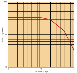
Fig. 3. For LVDS through cable, data rate capability varies with
cable length as shown in this graph for National Semiconductor's DS90LV017
driver IC.
Cost
LVDS saves cost by enabling a high level of integration. LVDS is commonly implemented on core CMOS processes, which greatly reduces the power dissipation of the devices. The CMOS approach allows for integration of multiple channels and digital glue or control logic on the same die without introducing thermal issues. As a result, these devices can be offered in standard IC packages that do not require heatsinking.
An example of such integration is provided by the Channel Link series of LVDS drivers and receivers from National Semiconductor. These devices perform high-speed parallel-to-serial and serial-to-parallel bus squeezing, converting a 21- or 28-channel TTL bus to a four- or five-channel LVDS link. These components greatly reduce system cost by shrinking the interconnect cable and connectors.
In addition, LVDS technology is scalable and compatible with system designs of the future. Existing 5- and 3.3-V devices will be interoperable–without level translation–with components operating at 2.8 V or lower. This capability ensures the viability of current designs, while easing the migration to new power supply systems.
Advertisement


