BY PAUL CASTILLO,
Applications Engineer,
Datatronics
www.datatronics.com
The layout of components in a switch mode power supply is a very important stage of the design process. A proper layout saves time during design verification and qualification phases. A power supply design with a proper layout requires smaller EMI filters or fewer filter stages. In this article, special consideration is given to the placement of magnetic devices in high frequency switch mode power supplies.
General layout guideline
The PCB must be partitioned according to circuit function and must flow from input to output as shown in Figs. 1a and 1b . Sensitive signal paths should be isolated from high power high frequency interference sources. The magnetic wire, as well as PCB traces, acts as transmitter/receiver antennas and they must be kept as short as possible. They should also be appropriately sized for current capacity and spaced apart according to voltage.

Fig. 1a: Switchmode power supply functional diagram

Fig. 1b: PCB partitioned by circuit function
EMI filter inductors
A typical electromagnetic interference (EMI) filter includes common mode inductors, differential mode inductors, and ‘X’ and ‘Y’ capacitors, Fig. 2. Differential mode capacitors (‘X’ caps) are placed across the input line; they are typically rated to 265 Vac 50/60 Hz with a capacitance value up to 2.2 µF. Common mode capacitors (‘Y’ caps) are placed from line to chassis ground and from neutral to chassis ground. They are rated up to 3,000 V to tolerate lightning strikes with a capacitance value up to 4,700 pF.
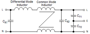
Fig. 2: EMI filter
EMI filter
Layout considerations
Effective layout of the devices is essential. The input power is typically from an ac-source operating at low frequency and flows directly through PCB traces and filter inductors onto the active devices. High frequency noise signals generated from the switching action of active devices flow back to the power source and other circuits in conducted and radiated forms.
It is important to select the smallest package for a given inductance that the input current will allow. The stray capacitance, together with the inductance, forms a tuned circuit and a self-resonant frequency that can reduce its effectiveness in the circuit.
PFC inductor
Switch mode power converters tend to draw current from the power line in a non-sinusoidal fashion. This results in current and possibly voltage distortions that can create problems with other equipment connected to the power grid and degrade the quality of the ac mains. This fundamentally requires the use of power factor correction or PFC.
There are two types of PFC: passive and active (see Figs. 3a and 3b ). A passive PFC is the simplest form of PFC. It uses a filter at the ac input to correct poor power factor. Only passive components are used for passive PFC, an inductor and some capacitors. Passive PFCs offer poor THD and are large and bulky because they operate at 50 to 60 Hz. Active PFCs are significantly smaller and lighter because they operate at higher switching frequencies. They provide better THD and are lower in cost than passive PFC circuits.
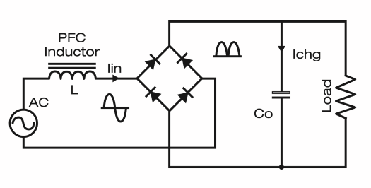
Fig. 3a : Passive PFC circuit
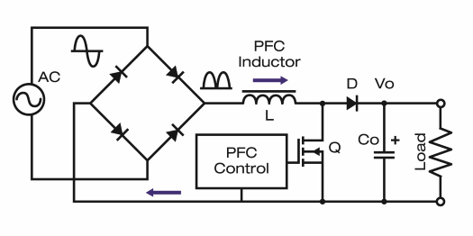
Fig. 3b Active PFC circuit
PFC inductor
Layout considerations
Keep the PCB trace length between the PFC inductor, the MOSFET drain and boost diode to a minimal length. Add an external shield made from an insulated copper foil to the PFC inductor and connect it to power GND. Keep the inductor away from sensitive control circuits to minimize RFI interference and heat radiation.
Power transformer
In terms of EMI and performance of switch mode power supplies the power transformer is the most critical and complex component. Its function is to transfer power from an external (ac) source to an external load. This function is accomplished by use of a ferromagnetic core and two or more isolated coils. Switching the rectified ac voltage across a primary coil induces a voltage on a secondary coil in proportion to the turns ratio, shown in Fig. 4 .
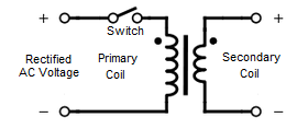
Fig. 4: Transformer primary and secondary coils
In switch mode power supplies, the switching frequency is many times higher than line frequency. The waveforms generally have a square wave shape which generate high frequency switching currents; and because of their shape contain harmonic elements at even higher frequencies. High frequency currents tend to flow primarily along the outer skin of the conductor which makes calculation of its cross sectional area more complex. The transformer will generate heat due to conduction losses in the windings, which are highest at full load.
Transformer
Layout considerations
The power path from the power switch to the primary winding and from the secondary winding to the diode must be kept as short as possible with minimum copper area. The copper area does need to be large enough to handle the currents and to help alleviate thermal issues in the semi-conductors.
Magnetic coupling from the magnetic flux can occur if an inductive component is placed close to the power transformer. This is particularly challenging in high density designs where space is limited. A magnetic flux band can be placed around the outside of the transformer and connected to ground to minimize the flux field.
Output inductor
The output inductor takes energy from an electric circuit and stores it in the form of a magnetic field and eventually returns the energy to the circuit. In a switch mode power supply, an inductor and capacitor form an LC filter which provides constant output voltage despite variations of the input voltage, Fig. 5 . The converter must regulate the output dc voltage within a specified range from light load to full load. The voltage delivered to the load must have low output ripple voltage and must be delivered with maximum efficiency.
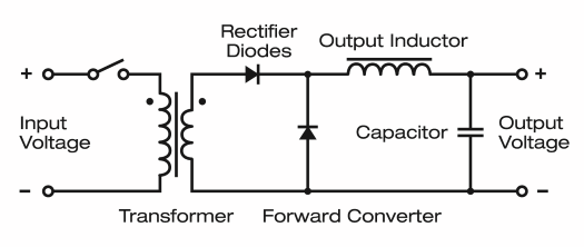
Fig. 5: Power supply with LC filter
Output inductor
Layout considerations
Because inductors form a link between magnetic and electric fields they are particularly susceptible to electromagnetic interference; they have an inherent ability to interact with magnetic fields. Shortening the signal traces and routing them parallel to their return path on adjacent layers reduces linking.
The output inductor must be placed close to the switching node of the output rectifier. The copper conductor pattern must be large enough to handle the current. Switching noise caused by eddy currents reduces the inductance value and they can be minimized by shortening the traces to reduce loop areas.
References :
1. AN1695/D Handling EMI in Switch Mode Power Supplies by: Ming–Hian Chew ON Semiconductor
2. PCB Layout Techniques of Buck Converter, No. 12027EBY05 Rohm Semiconductor
3. PCB Layout Guidelines Application Note AN-3185, CamSemi
4. Designing for Board Level Electromagnetic Compatibility, AN2321 Rev. 1, 10/2005 by T.C. Lun
Advertisement
Learn more about Datatronics


