Making LV energy harvesting practical: Part 2 – Integrating the ultra-LV booster module
Deciding whether to do the design work in-house using raw components or to interface a package solution isn’t always as simple as it sounds
BY BOB CHAO, CEO
Advanced Linear Devices
www.aldinc.com
This is the second of a three-part series about energy harvesting. You can find Part 1 at http://tinyurl.com/cte56d7
In today’s technologically advanced landscape, there exists a myriad of plug-and-play solutions for just about any application the designer is tasked to develop. Integrating a plug-and-play component has become an attractive alternative to a populated board design. However, as tempting as it may be to let others carry the burden of design and development, sometimes it just won’t work and integrating components is a better choice.
Overview
Because of the myriad of devices available that consolidate many functions, component manufacturers are becoming aware that their specific components may be integrated into products by designers who have little in-depth comprehension of their technology. This awareness is of particular benefit to designers or engineers across platforms of various disciplines — mechanical, chemical, civil, or specialized (nuclear, biological, nano, petroleum, etc.), needing to develop an interdisciplinary product.
Plug-and-play helps takes the design load off of engineers that must blend today’s disparaging technologies. Consider a manufacturer of wireless transmitters that may be asked to develop a particular harsh-environment seismic sensor that transmits data via a wireless link. This remote sensor might contain a digital sensor, an analog radio, and a power source. Such a product might incorporate designs that require digital, RF, and power engineering expertise. Perhaps the manufacturer is predominantly a radio-component-engineering firm and its analog engineers may not be comfortable integrating the digital and power designs from the ground up.
This is typically a scenario many of today’s manufacturers face. And, while there are any number of possible corollaries within these scenarios, the basic decision generally boils down to either designing and integrating all of the components from the ground up, or integrating existing drop-in modules.
Designing in the EH landscape
Today’s engineer faces a different model than their predecessors did during the earlier days of technology. While many modern applications can benefit from the “black box” drop-in-and-forget approach, unfortunately, emerging technologies, such an energy harvesting (EH), aren’t usually among them. This doesn’t mean that off-the-shelf modules won’t work in EH applications, just that there may be more of a learning curve in deciding the best approach especially in the ultra-low-power arena where requirements change quickly.
In the EH field, EH modules can be found in a wide arena of applications and across a wide platform of requirements within these applications. For example, sensors of every type and function are globally implemented in virtually every device known to man — from harsh and inaccessible remote physically installation to nanoimplantation in the human body. However, there are several EH sources that cannot supply sufficient energy for standard modules. This is where specialized devices, like low-voltage booster modules (LVBM), find a niche.
Integrating EH modules, LV booster
Typical off-the-shelf EH modules need to have at least 300 mV of input drive to function. There are currently some leading-edge modules that can cut that by about 30%, but that still puts the turn-on threshold too high for certain sources such as thermal electric generators (TEGs) and single photovoltaic sources. These sources typically put out power in the single- and double-digit power ranges (≈4 to 40 µW). For these applications, a booster module is the only option, and there is currently only one commercial product available.
A LVBM is designed to boost the ultralow voltages of the sources mentioned above, as well as other ultra-low-output devices. The module will “boost” the source’s native voltage or power output and produce an output capable of supplying the higher input threshold voltages required by EH modules (see Fig. 1 ). Without a LVBM, EH technology is unavailable to many applications that could benefit from it.
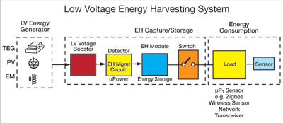
Fig. 1: The low-voltage booster module shown in a typical LV EH system.
LVBM — Design-in vs. drop-in
In the EH industry, the decision to design-in or drop-in depends on a number of factors, including the designer’s comfort with the technology, space availability, energy source, and application.
In many industry segments, the predominant driving force in the development of products is cost. Therefore, the first consideration to “design or drop” is to analyze the factors that affect the cost. Some of them are:
• How is the device available — components or module? What is the cost of the components vs. the module? Is there more than one form/fit/function option of the module/components? Is there in-house expertise available for design-in? If so, what is the design-in cost (time) of the component vs. the module, related to the cost of the expertise? What are the extended costs producing the product with a module vs. the components (production, material, and manufacturing)?
There are other factors as well that may need to be evaluated in the overall cost equation, such as origin of manufacture and the distribution chain.
The design-in side
In the case where there is both a drop-in module and a component kit, one argument for design-in of the LVBM generally relates to the complexity of the device design itself, and the complexity of the design-in circuit. In most cases, if the product design is very complex or needs to have tolerances precisely controlled, it is more likely that the manufacturer will want to control all of the component parameters.
Other arguments for using the LVBM components relate to available board real estate and the manufacturing process. If the critical parameter for the end product revolves around footprint, then the solution is to design-in the raw components of the LVBM. This is particularly applicable with space constrained application such as biometric sensors in body sensors. Device concealment in security applications is another area where the sensor must be as inconspicuous as possible. Both of these applications place a priority on device footprint.
The power, circuit placement, and the electromagnetic Interference/radio frequency interference (EMI/RFI) demands of the design-in will have to be evaluated as well. So will the circuit input/output (I/O) interconnect parameters and board layout. Finally, the overall package design is also a technical consideration. All of this needs to be assessed for its impact on non-recurring engineering (NRE) costs and what effect they have on the final design.
Finally the manufacturing process itself should be determined. If the product is expected to have high volume and long life, it is generally cheaper, over the long run, to manufacture with integrated design-in components.
The drop-in module side
As a drop-in black box, the LVBM’s most significant advantage is the cost of integration. The LVBM has a two-wire input and a two-wire output (see Fig. 2). All the product manufacturer really needs to know to integrate it is the device’s power requirements and the I/O impedances. This means that virtually any engineer with minimal electronics training can integrate the unit, electrically. This approach also minimizes NRE costs. However, the drop-in approach requires design considerations for all of the issues that come with adding a module — location, housing, fixed or removable, and environmental standards.
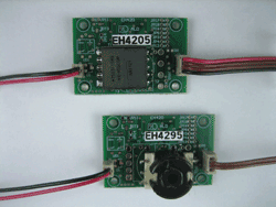
Fig. 2: Low-voltage booster modules
In almost all cases, the cost of integrating components into a module makes it more expensive. Depending upon circumstances, the additional cost of simple black-box integration can turn out to actually be less expensive than its component counterparts. In such cases where serviceability is a consideration, or the product is not expected to have high volume or the cost of component integration cannot be amortized, modules are the preferred choice.
Another consideration is time to market. If this is a critical factor, the extra cost of the drop-in design can be weighed against the potential loss of market share or sales by a release delay. Finally, if field serviceability is a device criterion, modular designs typically offer a much easier service route if that is part of the product concept.
This second installment of the article series has addressed some of the issues that product manufacturers face when developing and producing EH devices. Because EH products have a wide application base, each individual application has unique design issues. The low-voltage booster module is a particular device for specific conditions in some EH applications. There are persuasive arguments for both integration methods either as drop-in modules or as individual components. Prudent designers allow the application and manufacturing requirements to determine the best route to address their EH needs.
Of course, there are any numbers of other considerations that can weigh in on either side of the argument. But as is generally the case, the application calls the shots and the prudent designer must examine all the angles. ■
Advertisement
Learn more about Advanced Linear Devices


