Advanced CMOS process technologies enable IC designers to deliver higher performing devices, but also increase the need for extra board-level ESD protection to ensure the reliability of the end product
BY ROBERT ASHTON, Ph.D.
Sr. Protection & Compliance Specialist
ON Semiconductor
Phoenix, AZ
www.onsemi.com
Advances in CMOS technology have allowed semiconductor suppliers to produce integrated circuits (ICs) with increasingly small features sizes. Smaller IC feature sizes have numerous advantages. Smaller features allow more circuits to occupy smaller areas, facilitating ICs with more features in a smaller silicon area at a lower cost per IC. CMOS transistors with smaller features also have higher performance.
The result is the win-win-win situation of more features, with higher performance, at lower cost. CMOS process geometries have shrunk dramatically; while mature 0.18- or 0.13-µm processes can be a cost-effective choice for custom analogue/mixed-signal ASIC projects, leading-edge digital IC designs are targeting geometries such as 45, 32, and even 28 nm.
A side effect of smaller geometries is the requirement for lower operating voltages. Failure to lower IC operating voltages would lead to gate oxide failures and other reliability issues such as transistor aging. Lower voltages have positive and negative aspects.
On the positive side, lower voltages result in lower power dissipation, a major advantage for today’s popular battery-powered handheld electronics. On the negative side there are a number of electronic design challenges such as reduced dynamic range and lower signal to noise ratios which accompany the lower supply voltage.
Additionally, the electrical stresses that electronic devices from computers to mobile phones are susceptible to, such as electrostatic discharge (ESD), have not changed in voltage or current magnitudes as IC technologies have advanced.
The result is that lower-voltage ESD events can now damage state-of-the-art ICs. This has implications in how electronic systems are designed to withstand ESD.
To understand these implications, it is necessary to understand how ESD protection is included in circuit designs. The principles of ESD design are similar at the IC level and at the system level, so we will start with a discussion of protection at the IC level and then expand to system level. We will then learn how on board ESD protection and proper board design are important tools in system-level ESD design.
All electronic components and circuits have an intended operating voltage range, as well as a safe guard band as illustrated in Fig. 1 . Voltages beyond this guard band will initiate circuit damage. As advanced process technologies demand lower operating voltage, the guard band region is narrowing.
ESD protection devices are used to maintain voltages within the guard band region during ESD stress. As the guard band region shrinks, there is a need for ESD protection devices with lower on-state resistance so that voltages stay within the guard band region. Protection against overvoltage is typically implemented using a device that clamps the voltage within the guard band region by providing a low-impedance path. This is illustrated by the voltage clamp in Fig. 1.
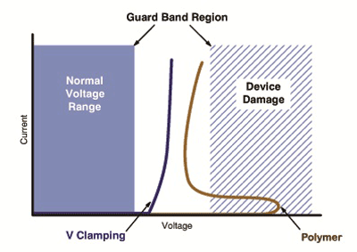
Fig. 1: Operating-voltage regions for ICs and ESD-protection devices.
Samples of on-chip ESD design for I/O pins are shown in Fig. 2 . On the left of Fig. 2, voltage clamps are placed on the input pin to turn on and provide a low resistance path to the IC’s ground bus if the voltage exceeds the normal voltage range. This protects the sensitive receiver from excess voltage and current. These clamps can be single zener diodes, back to back zener diodes as shown in the figure, or specially designed snapback structures formed from nMOS transistors.
A second popular approach is the use of steering diodes and a power supply clamp as shown on the right side of Fig. 2. A negative stress on the I/O with respect to ground will pass through the steering diodes to ground, preventing stress on the input gates. A positive stress with respect to ground will pass through the steering diodes to VDD and on to the power rail.
A power supply clamp between VDD and GND will then conduct the stress current from the VDD bus to ground. The power supply clamp could be a simple zener diode or an active circuit that detects unexpected voltages between VDD and GND and turns on a large transistor between VDD and GND to provide a low impedance path. This circuit works similarly for stress between the I/O and VDD .
The two sets of steering diodes and the resistor on the right side of Fig. 2 are part of a strategy called primary and secondary protection. The primary protection is the set of diodes closest to the I/O pin and is intended to carry most of the stress current.
The secondary protection is the set of diodes closest to the sensitive MOS transistor gates. Some stress current will flow through the secondary protection but the resistor will not only help limit the current to the secondary protection but the voltage drop over the resistor will also help turn on the primary protection. This kind of strategy will be seen again when discussing system-level protection.
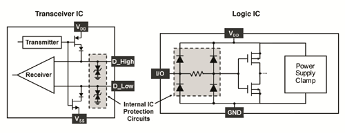
Fig 2: Typical internal ESD protection circuitry.
A major difference between ESD design for safe handling of ICs and ESD design of systems is in the magnitude of the stress. The ESD protection built into most ICs is intended to ensure that the IC can be handled with high yield in an ESD controlled production facility, where ESD events are rare and of low intensity.
Today the ESD targets for state of the art ICs are 1,000-V HBM and 250-V CDM. The peak current for 1,000 V HBM is approximately 0.67 A with a 150 ns decay time while CDM currents can be several amps but last just a couple of ns. This compares with peak currents of 30 A with a characteristic time of about 50 ns for a typical 8 kV stress according to IEC 61000-4-2, the standard most commonly used to test systems for robustness from ESD. It is clear that the input and output pins of a state-of the art integrated circuit cannot survive a system-level ESD pulse without special design considerations.
If the difference between ESD test and design of ICs for safe handling and ESD testing and design at the system level is largely a matter of magnitude, why not just design system-level ESD robustness into I/O pins that actually connect to system-level I/Os such as USB, Ethernet, HDMI, and Display Port? In some cases this is possible, but not often wise.
ESD protection structures cannot be scaled to smaller area due to the availability of smaller geometry features. System-level ESD currents are high and do not scale down for newer generations of technology. Roughly the same silicon area is needed to design a system level ESD structure in a state of the art technology as in a more mature technology. The cost of that area is much higher in the newer technology, so that the cost of system-level ESD protection goes up as the technology gets more advanced. Additionally, for high-speed data lines it is necessary to maintain very low capacitance in the protection design. This can be very difficult in the most advanced technologies, which typically have very high silicon doping levels, which result in high capacitances. The use of ESD protection placed on the circuit board, such as the TVS device shown in Fig. 3 , therefore, becomes very desirable.
ESD protection devices
System designers can choose from a number of protection product alternatives, depending on the application and type of overstress expected.
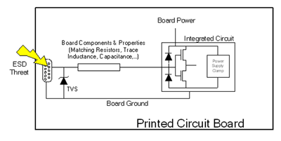
Fig. 3: Example of on board ESD protection placed on a printed circuit board.
An example is the metal-oxide varistor (MOV). An MOV responds quickly to transients but their high capacitance places significant extra loading on signal lines. Thyristor surge protection devices (TSPD) are often used for protection in telecom and Ethernet equipment to protect against surges due to their high current-carrying capability, but they are usually too slow and have turn on voltages which are too high to be effective for ESD protection.
Polymer ESD protection devices are sometimes used on very-high-speed data lines due to their low capacitance, but they typically have very high turn-on voltages and their clamping voltages are often several times the voltage that modern integrated circuits can withstand. Polymer IV characteristics are shown in Fig. 1. In the majority of low- to medium-power applications, the silicon-based transient voltage suppression (TVS) diode is the device of choice for ESD protection.
TVS diodes
The use of a TVS product is illustrated in Fig. 3. The TVS product is placed close to the IO connector. In an ideal situation the TVS device will turn on before the IC’s internal circuit and direct the entire surge current to ground. In practice there will often be a sharing of current between the TVS product and the ESD protection structures built into the IC. This arrangement is very similar to the discussion of primary and secondary protection in on chip ESD protection as discussed earlier and shown in Fig. 2. TVS products placed on the board have an advantage over on chip ESD protection because the board properties such as trance inductance and matching resistors can be used as part of the ESD protection strategy, limiting ESD current flow to the IC and providing extra voltage drops which help turn on the primary, on board ESD protection device. ON Semiconductor makes a wide variety of TVS products for a variety of applications and designed to have industry leading low clamping voltage.
Diode based TVS products have an advantage over MOV and polymer based ESD protection products. MOVs and polymers always have symmetric properties for positive and negative stress. TVS devices can be designed with both symmetric and asymmetric properties. Single zener diodes have an asymmetric property, conducting as a forward bias diode in one polarity and as a zener breakdown diode in the opposite polarity. This is ideal for protecting circuit nodes which have only a single polarity such as 0 to 3.3 V. Back-to-back diodes provide symmetrical response, conducting with a series combination of forward and zener breakdown conduction for both positive and negative polarities. This is ideal for protecting circuit nodes which are symmetrical about 0 V such as –3.3 to +3.3 V.
Using power supply decoupling
ESD protection arrays can incorporate power supply decoupling capacitors into the protection strategy. At ESD frequencies the µF range ceramic decoupling capacitors between power and ground represent a low impedance path to ground. Steering diodes in a TVS array can direct the ESD current to power and ground lines on the board, significantly reducing voltage transients on the board as shown in Fig. 4 .
Zener diodes within the TVS array further limit voltage transients. Zener diodes built into the array package will also have very low inductance and will therefore be very effective at eliminating inductive voltage spikes which can occur during an ESD event. To be effective the board-level capacitance needs to be close to the TVS array and both the TVS array and capacitors need to be positioned to avoid any high impedance connections such as long narrow traces. ON Semiconductor makes TVS array products suitable for many applications. Many are aimed at specific applications and are designed for easy board placement.
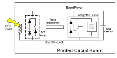
Fig. 4. Example of a TVS array and decoupling capacitors being used as part of an ESD protection strategy.
Protecting high-speed data lines
When TVS diodes are used to protect high-speed data lines, the associated capacitance will cause disturbances to the signals resulting in a loss of data integrity. The eye diagrams of Figs. 5 and 6 , which compare a USB 2.0 signal line with no protection and with a TVS diode of capacitance 65 pF, illustrate how the capacitive loading imposed distorts signal transitions. The traces crossing the USB 2.0 mask in demonstrate unacceptable signal integrity when a high capacitive loading is added. Designers must identify ESD protection solutions that can protect the sensitive lines without adding signal degrading capacitance.
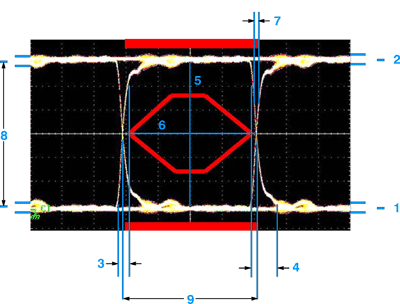
Fig 5. Eye diagram for USB 2.0 data line with no ESD protection applied.
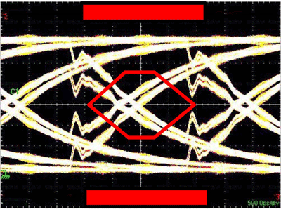
Fig. 6: Eye diagram for USB2 .0 data line with 65pF ESD protection diode.
Figure 7 shows the USB 2.0 high-speed signal with ON Semiconductor's high-speed TVS diode, ESD9L, which has ultra-low capacitance of 0.5 pF. The eye diagram reveals no major changes in the mean values of logical 1 and 0, or in the signal rise and fall times, showing that the device has negligible adverse effect on data integrity.
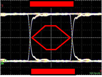
Fig. 7: Eye diagram for USB 2.0 data line protected by ON Semiconductor ESD9L TVS diode of 0.5-pF capacitance.
Assessing ESD performance
The ESD properties of electronic components can be characterized using transmission line pulse (TLP) measurements. The standardized 100-ns pulse length and currents up to 40 A used in TLP closely match the pulse lengths and currents that occur in ESD events. TLP is applicable for IEC 61000-4-2 system-level ESD, as defined by, and ANSI/ESDA/JEDEC JS−001−2011 device-level Human body model (HBM) tests.
A TLP system can be used to produce I−V curves in which each data point is from a pulse whose duration and current amplitude are in the same range as system-level ESD events. These I−V curves, and parameters derived from them such as dynamic resistance and voltage intercept, can be used to compare the properties of different TVS devices and can be used to predict device performance in a circuit.
Conclusion
The latest CMOS fabrication technologies enable many advances in IC performance, such as reductions in die size, operating voltage, and power consumption, as well as improvements in speed and functionality.
Although design rules are shrinking, ESD voltages remain unchanged and so present an increased threat to today’s highly sensitive devices. Plentiful application guidance and a broad selection of dedicated protection devices, including low-capacitance devices for high-speed applications, provide designers with the tools they need to create robust products capable of meeting the toughest stress-testing criteria. ■
Advertisement
Learn more about ON Semiconductor


