The MAX 10 is Altera’s latest family of low cost FPGAs optimised to capture the advantages of CPLD and FPGA capability in a single package. Building on the best of both worlds, MAX 10 is enhanced with features that enable the next level of cost effective integration – the perfect core for any smart device connected to the cloud. Although packed with sophisticated features and optimised to enable the efficient implementation of embedded products, the MAX 10 is surprisingly simple to use in design. Engaging in a MAX 10 development is easy thanks to the ready availability of versatile development kits, example designs and a strong user community.
MAX 10 reduces cost and size in a number of key areas:
• Internal flash for FPGA image and software memory.
• A 32bit NIOS2 processor softcore eliminates the need for a separate processor.
• Remote upgrade capability eliminates the need for a separate configuration controller.
• An integrated watchdog timer eliminates the requirement for an external device.
• An internal 232MHz oscillator and flexible PLLs eliminate the need for an external clock.
• A single power supply option reduces PCB board layers and the need for multiple regulators.
• Integrated multichannel, 12 bit SAR ADC can remove the requirement for an analog converter.
• An integrated temperature sensing diode eliminates the need for a separate temperature sensor.
• Versatile I/O ring reduces voltage level translator and passive component requirements.
Internal flash is a huge advantage for MAX 10 FPGAs, but it does not stop there as Altera has included a number of useful features to enable its full use in products. FPGAs typically require a power up time period to read their image from an external memory. MAX 10 features instant power up from one of several internal configuration flash arrays that provide a dynamic fail-safe remote upgrade. A watchdog timer can be enabled to monitor remote flash configuration with automatic fall back to a previous image if unsuccessful. Multiple flash arrays are incorporated for program and data storage to eliminate the need for external, non-volatile memory in many applications.
The MAX 10 reduces power supply cost and size with a single 3.0-3.3V power supply option thanks to an integrated voltage regulator. A high efficiency dual supply device option is also available. The versatile I/O ring can support many single and differential I/O standards including 3.3V LVTTL/LVCMOS. When combined with independent I/O bank voltage capability, separate level translating buffers are avoided. Every I/O element has an option to configure a Schmitt trigger input buffer to provide noise immunity and switch debouncing. Each I/O block contains two output enabled registers that can operate in DDR mode for high speed serial bus and memory interfaces. Outputs that have the capability of being open drain with optionally enabled internal pull up resistors with a configurable slew rate control and a programmable current strength are able to drive up to 16mA for some interface standards.
Analog blocks containing multichannel ADCs, a temperature sensing diode and an integrated 232MHz internal ring oscillator round off a powerful architecture. When combined with PWM or delta sigma converters and Altera’s DSP Builder the MAX 10 FPGA can be used at the heart of monitoring and control applications requiring analog-to-digital conversion and signal processing. Thanks to TMSC 55nm NOR Flash technology, Altera’s rich heritage of intellectual property and a powerful development ecosystem, designers have ready access to the device’s flexible FPGA fabric.
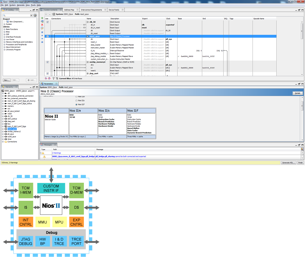
This incorporates DSP blocks, LPDDR2/DDR3 interface capability, PLLs, up to 50K LEs and 1.6Mbits of block RAM. Central to Altera’s easy to use IP is the Qsys System Integration tool that enables developers to define a system architecture that instantiates a wide variety of interoperable softcore modules. This includes the world’s most versatile embedded processor – the 32bit NIOS II.
Figure 1: Qsys System Builder and the NIOS II Architecture
Start Immediately with a Development Kit!
Developments kits simplify the design process, enabling a way to rapidly develop the FPGA design and embedded software on a well-documented reference platform. Many kits are available, optimized for a wide range of applications. Basing the underlying hardware architecture on tried and tested elements of reference designs enables the use of working example projects as starting points – speeding development and mitigating risk. Development timeframes can be accelerated by combining this strategy with the wide variety of available operating systems with development kit specific BSPs, integrated networking stacks and device drivers.
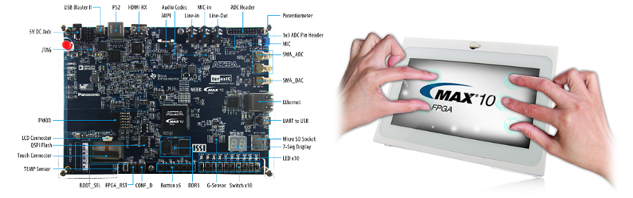
The Terasic NIOS II Embedded Development Kit (NEEK) has everything required to create a full processor-based system. It is an integrated platform with a number of reference designs that focus on a range of applications. The kit is optimized to enable rapid design of customized solutions for embedded processing applications, multimedia interface products, human-machine interfaces and video display. The kit features a capacitive LCD multimedia color touch panel with native support of multi-touch gesturing. It also incorporates an eight megapixel image sensor, a light sensor and a three-axis accelerometer. Demonstration reference designs include robotic control, HDMI Rx, sensing, audio and camera interfacing.
Figure 2: Terasic MAX 10 NIOS II Embedded Development Kit
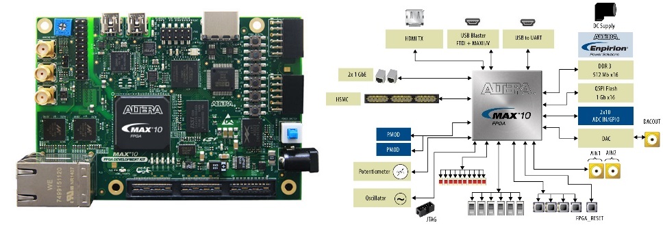
The Altera MAX 10 FPGA Development Kit is optimized for a wide variety of applications including HDMI and industrial Ethernet designs. An embedded Linux reference design is available for the NIOS II processor with strong online community support. The development kit includes interfaces to daughter cards and peripherals using HSMC and Digilent Pmod™ compatible connectors and has inbuilt monitoring of FPGA power using the power monitor graphical user interface (GUI). The board is well documented, open and reusable as a proven platform to base a design upon.
Figure 3: Altera MAX 10 FPGA Development Kit
The MAX 10 FPGA Evaluation Kit is a low cost entry-level board with integrated FPGA power supply monitoring and an adjustable I/O bank voltage to enable level translation. The board utilizes an Altera Enpiron power supply and enables access to FPGA’s flash memory, ADC interfaces and the digital I/O ring. The kit is incredibly flexible due to an integrated Arduino UNO R3 interface connector that enables connection to compatible Arduino Shields. This enables thousands of peripheral boards containing functionality like sensors, motor controllers, GPS and wireless transceivers. The kit’s PCB board and schematic are well documented and available as a model for designs.
Figure 4: MAX 10 FPGA Evaluation Board
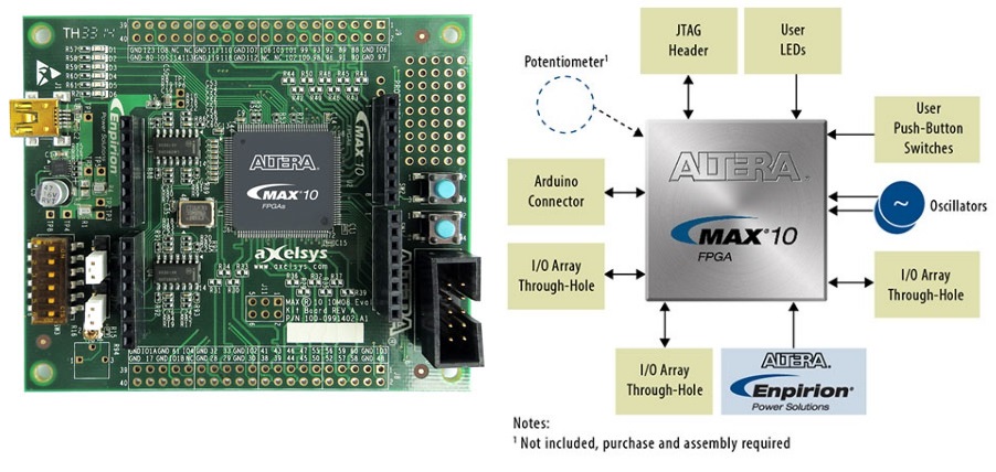
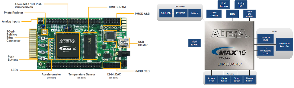
The BeMicro MAX 10 is a tiny development kit available from Arrow that enables designers evaluate and utilize the MAX 10 for embedded applications. It includes an Enpiron power SoC, 8Mbytes of SDRAM, an accelerometer, LEDs, pushbuttons and expansion connectivity. The expansion headers include two 6-pin PMOD and two 4- pin prototyping headers along with an 80-pin card edge connector. Users can directly interface development tools via the inbuilt USB Blaster port. The board is well documented with a Getting Started User Guide for accelerating design and is perfect as a low cost prototyping platform for rapid development.
Figure 5: BeMicro MAX 10
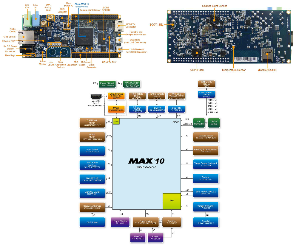
The DECA MAX 10 Development Board from Arrow is small but is a powerful, highly versatile and robust development platform. It incorporates DDR3 memory, Ethernet, gesture light sensing, HDMI Tx, audio line in or out, microSD socket and two SMA inputs for the MAX 10 ADCs. The DECA system comes complete with a BYD camera and WiFi-BLE wireless interface modules that plug into the boards two 46-pin BBB expansion headers. Developers can make full use of Arrow’s BLE/WIFI BeagleBone compatible cape that showcases Texas Instrument’s families of BLE and Wi-Fi solutions. Developers can also use the camera module to capture 8M-pixel CMOS images using a MIPI video input interface.
Figure 6: DECA MAX 10 Development Board
Give it a Go Today!
Developing a system based upon an embedded FPGA has never been simpler. MAX 10 offers levels of integration that truly enable significant cost savings and levels of integration not before seen. A plethora of development kits with Operating System BSP support and access to peripheral expansion for sensing and network connectivity enable using the MAX 10 in applications that would have previously required more complex and expensive microcontrollers. The introduction of dynamic image and user flash upload via a UART interface with watchdog and failsafe fall back future-proofs designs by facilitating upgrade and support. Hardware development risk is mitigated through well documented robust solutions and software is accelerated through access to many reference designs and a strong user community. FPGA design tools include free web based options. Software development and debugging is made easy using the Altera software development environment based upon Eclipse. Talk to an Altera representative about how they can get you started today!
Advertisement
Learn more about Altera


