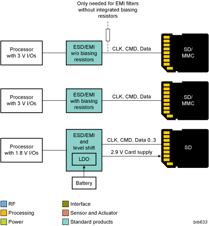
The SD-memory card and MMC are the most popular memory cards in today’s communication, computer and consumer appliances. They are designed to support state-of-the-art security and capacity requirements demanded by audio and video applications.
According the IEC61000-4-2 standard, SD host interfaces require an additional high-level ESD protection, in addition to the integrated ESD protection which is typically very weak. Other strict EMI regulations and system requirements, as specified in GSM mobile phones, strongly request filters that reduce the radiated/conducted EMI. However, they must still comply with the electrical requirements of the interface specification.
The continuing trend of miniaturization of portable appliances implies that interface devices offering ESD protection and EMI filtering should also integrate biasing circuits/resistors into a single small-sized package. NXP’s memory card interface solutions fully support this continuing trend and offer interface conditioning functions such as:
• High-level ESD protection according the IEC61000-4-2 standard, often exceeding the highest specified level 4
• EMI filtering, suppressing unwanted Radio Frequencies (RF), in combination with SD interface compliant physical signaling
• Integrated biasing resistor networks to reduce the component count and to free up additional space on the Printed-Circuit Board (PCB) surface
• A regulated power supply to supply SD-memory cards directly from e.g. a battery
• Voltage level translation to enable the use of low-voltage host processors to communicate with 2.7 V to 3.6 V compliant SD-memory card devices
For additional information, download application note
Download Full Block Diagram Below
Advertisement

Learn more about NXP Semiconductors


