What are MEMS?
Microelectromechanical systems (MEMS), also known as microsystems technology in Europe, or micromachines in Japan, are a class of devices characterized both by their small size and the manner in which they are made. MEMS devices are considered to range in characteristic length from one millimeter down to one micron – many times smaller than the diameter of a human hair.
MEMS will often employ microscopic analogs of common mechanical parts and tools; they can have channels, holes, cantilevers, membranes, cavities, and other structures. However, MEMS parts are not machined. Instead, they are created using micro-fabrication technology similar to batch processing for integrated circuits.
Many products exist today that use MEMS technology, such as micro heat exchangers, ink jet printer heads, micro-mirror arrays for high-definition projectors, pressure sensors, infrared detectors, and many more.
Why do we want MEMS?
Microelectromechanical systems (MEMS), also known as microsystems technology in Europe, or micromachines in Japan, are a class of devices characterized both by their small size and the manner in which they are made. MEMS devices are considered to range in characteristic length from one millimeter down to one micron – many times smaller than the diameter of a human hair. MEMS will often employ microscopic analogs of common mechanical parts and tools; they can have channels, holes, cantilevers, membranes, cavities, and other structures. However, MEMS parts are not machined. Instead, they are created using micro-fabrication technology similar to batch processing for integrated circuits. Many products exist today that use MEMS technology, such as micro heat exchangers, ink jet printer heads, micro-mirror arrays for high-definition projectors, pressure sensors, infrared detectors, and many more.
“They tell me about electric motors that are the size of the nail on your small finger. And there is a device on the market, they tell me, by which you can write the Lord's Prayer on the head of a pin. But that's nothing; that's the most primitive, halting step in the direction I intend to discuss. It is a staggeringly small world that is below. In the year 2000, when they look back at this age, they will wonder why it was not until the year 1960 that anybody began seriously to move in this direction.”
–Richard Feynman, “There's Plenty of Room at the Bottom” December 29th 1959 at the annual meeting of the American Physical Society at the California Institute of Technology (Caltech)
In this classic and somewhat prophetic lecture, “There's Plenty of Room at the Bottom,” Richard Feynman goes on to describe how we might write out every volume of Encyclopedia Britannica on the head of a pin. But we might wonder: why would one want to manipulate objects on such a minute scale?
MEMS devices perform many of the same tasks as macroscopic devices while also offering many advantages. The first and most obvious of these is miniaturization. As previously mentioned, MEMS-scale devices are small enough to be manufactured in a batch fabrication process, similar to the ICs of today. And as with the IC industry, batch fabrication can significantly reduce the costs of mass production. MEMS also, in general, require a much smaller amount of material to produce, which can further reduce costs.
In addition to the prospect of being cheaper, MEMS devices can also be more applicable than their much larger equivalents. Designing metal ball and spring accelerometers into smartphones, cameras, airbag control units, or similarly small sized devices would be impractical at best; by reducing device size by several orders of magnitude, MEMS can be used in applications where a conventional sensor would be far too large.
Ease of integration is yet another advantage of MEMS technology. Because they are fabricated with similar processes used in fabricating ASICs, MEMS structures can be more readily integrated with the microelectronics. Integration of MEMS and CMOS structures into a truly monolithic device has proven to be highly challenging, however much progress continues to be made. Meanwhile, many manufacturers have employed a hybrid approach to create commercially successful and cost-effective MEMS products.
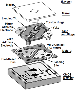
The Texas Instruments Digital Micro Mirror Device (DMD) is one such example. DMD is the core of TI’s DLP® technology, which is widely used in projector units ranging from business and classroom models to digital cinema. Each 16µm square mirror is actuated electrostatically by a voltage potential between it and the CMOS memory cell below it. Grayscale images are produced by pulse-width modulating the mirrors between on and off states. Color is added either by using a three-chip solution (one chip for each primary color), or with a single chip and a color wheel or RGB LED light source. Designs using the latter technique synchronize the DLP chip with the rotation of the color wheel, displaying each color in quick succession so that the viewer sees a single full-spectrum image. 
Perhaps one of the most interesting features of MEMS is the designer’s ability to exploit the peculiar physics that emerge from such a small-scale physical domain – a topic which will be revisited later.
MEMS today
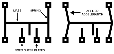
For these reasons and more, many MEMS products are commercially quite successful, with many devices already in widespread use. The automotive industry is among the main drivers behind MEMS technology. MEMS vibrating structure gyroscopes, for example, are new and fairly inexpensive devices currently used for automotive anti-skid or electronic stability control systems. The Murata Electonics Oy SCx-series of MEMS accelerometers, gyroscopes, and inclinometers and various combinations of these functions reside on a single chip to enable specific automotive applications, where precision is required in confined spaces. MEMS-based airbag sensors have universally replaced mechanical type crash sensors in nearly all cars made since the 1990s. Figure 2 shows a simplified example of a MEMS accelerometer similar to what might be used as a crash sensor. A cantilever beam with proof mass is attached to one or more fixtures that act as springs. When the sensor is accelerated along the beam’s axis, the beam is shifted some distance, which is measured as a change in capacitance between the beam “teeth” and the fixed outer conductors.

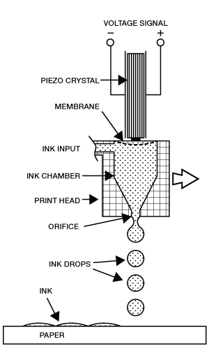
Many commercial and industrial inkjet printers use MEMS based technology in printer heads to withhold ink drops and precisely deposit them only when needed – a technique called Drop-on-Demand (DoD). An ink drop is placed by applying a voltage potential across an element composed of piezoelectric material, such as lead zirconate titanate, causing it to deform. This increases the pressure within the ink chamber of the printer head, forcing a very small amount of the (relatively incompressible) ink out of the nozzle. 
Meanwhile, other MEMS technologies are only just beginning to enter the market on a large scale. Micromachined relays (MMRs), such as those developed by Omron, offer a class of relays that are faster, more efficient, and capable of an unprecedented degree of on-chip integration. Omron has also brought their MEMS expertise to bear on temperature sensors with their new D6T non-contact MEMS thermal sensors. The D6T integrates ASIC and thermopile elements in a MEMS fabrication process, resulting in a miniaturized non-contact thermal sensor measuring only 18 x 14 x 8.8mm (4×4 element type).
Of course, the MEMS technology of today is not limited to single-sensor devices. Why should it? Consider the human senses: a single eye gives us color, motion, and (some) positional information, while two eyes enables binocular vision for improved depth perception. In fact, many of our perceptual experiences require a combination of senses in order to be meaningful at all. The idea is that by combining sensory data we can compensate for the weaknesses and drawbacks of each individual sense organ, and arrive at an understanding of the environment that is in some way superior. In the human context, this is called “multimodal integration”; in electronics it’s called sensor fusion. Sensor fusion, especially as it relates to MEMS, is an important development in sensor technology for mobile devices. Many manufacturers are already offering complete solutions, such as Freescale with their 12-Axis Xtrinsic Sensor Platform for Windows® 8. This platform integrates a 3-axis accelerometer, 3-axis magnetometer, pressure sensor, 3-axis gyroscope, and ambient light sensor with a ColdFire+ MCU for a total hardware solution – then couples it with proprietary sensor fusion software.
The MEMS market continues to pick up pace as the advantages of MEMS devices gain recognition. According to Yole Développement’s 2012 MEMS industry report, MEMS “will continue to see steady, sustainable double digit growth for the next six years”, becoming a $21 billion global market by 2017.
MEMS design and manufacturing
“It is interesting to consider what the problems are in such small machines. Firstly, with parts stressed to the same degree, the forces go as the area you are reducing, so that things like weight and inertia are of relatively no importance. The strength of material, in other words, is very much greater in proportion. The stresses and expansion of the flywheel from centrifugal force, for example, would be the same proportion only if the rotational speed is increased in the same proportion as we decrease the size.”
–R. Feynman, “There's Plenty of Room at the Bottom”
Scaling and Miniaturization
Introductions to the design and manufacture of MEMS often begin with a review of scaling and miniaturization. If we ask, for example, why one cannot simply take an air compressor or a ceiling fan and shrink it down to the size of a flea, the answer is scaling laws. A flea-sized ceiling fan will not behave in the same way as a normal-sized fan 1000 times larger, because the involved forces change in strength relative to each other. The scale factor, S, can aid in understanding how.
Consider the area of a rectangle, equal to the product of its length and its width; if the rectangle is scaled down by a factor of 100 (i.e. length/100 and width/100 ) , the rectangle area shrinks by a factor of (1/100)2 = 10,000. Therefore, the area scales as S2. Likewise, volume scales as S3 – so it follows that at increasingly smaller scales, surface (area) effects have greater impact than volume effects.
Carefully considering the scale factor of different forces can reveal which physical phenomena are most relevant at a given scale. Force due to surface tension scales as S1, pressure and electrostatics related forces as S2, magnetic forces as S3, and gravity scales as S4. This helps explain how water striders (or “water bugs”) can walk on water, and why a pair of ball bearings do not behave like a binary star system. Scale factors can also guide our understanding of how to design MEMS-sized devices, although developing a full mathematical model is eventually necessary in any design.
Subsystem Modeling
Introductions to the design and manufacture of MEMS often begin with a review of scaling and miniaturization. If we ask, for example, why one cannot simply take an air compressor or a ceiling fan and shrink it down to the size of a flea, the answer is scaling laws. A flea-sized ceiling fan will not behave in the same way as a normal-sized fan 1000 times larger, because the involved forces change in strength relative to each other. The scale factor, S, can aid in understanding how. Consider the area of a rectangle, equal to the product of its length and its width; if the rectangle is scaled down by a factor of 100 (i.e. length/100 and width/100 ) , the rectangle area shrinks by a factor of (1/100)2 = 10,000. Therefore, the area scales as S2. Likewise, volume scales as S3 – so it follows that at increasingly smaller scales, surface (area) effects have greater impact than volume effects. Carefully considering the scale factor of different forces can reveal which physical phenomena are most relevant at a given scale. Force due to surface tension scales as S1, pressure and electrostatics related forces as S2, magnetic forces as S3, and gravity scales as S4. This helps explain how water striders (or “water bugs”) can walk on water, and why a pair of ball bearings do not behave like a binary star system. Scale factors can also guide our understanding of how to design MEMS-sized devices, although developing a full mathematical model is eventually necessary in any design.
Models are especially needed for MEMS designs due to the non-intuitive nature of sub-millimeter devices. Generally, an entire microelectromechanical system is too complex to model analytically as a whole, so it is usually necessary to break the model into subsystems.
One way of doing this is to categorize parts by function, such as sensors, actuators, microelectronics, mechanical structures, etc. Lumped element modeling uses this approach, representing physical parts of the system as discrete elements with idealized characteristics. Electronic circuits are modeled the same way, using idealizations of resistors, capacitors, diodes, etc. of various complexities. We understand that, when possible, electrical engineers will graciously use the much simplified Kirchhoff's circuit laws rather than Maxwell’s equations to model a circuit.
Again, as with electronics, the system can be modeled even more abstractly using block diagrams. At this level it becomes convenient put aside the physicality of each element and instead describe the system in terms of transfer functions. This results in a MEMS model that is much more conducive to control theory techniques – an important set of tools for most high performance designs.
Design Integration
Whereas standard IC designs are often implemented as a series of discrete steps, MEMS design is much different; the design, layout, materials, and packaging of MEMS are inherently intertwined. Because of this, MEMS design can be more complex than IC design – often requiring the simultaneous development of every design “phase”.
MEMS packaging is the process that diverges perhaps most widely from the CMOS design. MEMS packaging is meant primarily to protect the device from environmental damage while also providing an interface and mitigating unwanted external stress. MEMS sensors often use stress as a means of measurement; excessive stress can impair functionality by deforming the device and inducing sensor drift.
The packaging requirements for a given MEMS design are often unique and the package must be designed specifically for that device. In the industry it is well known that packaging can account for a huge portion of the total product cost – in some cases exceeding 50%.
There is no single standard for MEMS packaging, and only recently have any sort of packaging technologies emerged, among these being MEMS wafer-level packaging (WLP) and through-silicon via (TSV) techniques.
Fabrication
Taking from microelectronics, the strength of MEMS fabrication is the batch process. Mass production adds economy of scale to MEMS devices just like it does any other product. As with IC fabrication, photolithography methods are often the most cost-efficient and certainly the most common technique. However, other processes, both additive and subtractive, are indeed used as well, including chemical/physical vapor deposition (CVD / PVD), epitaxy, and dry etching.
Materials used in MEMS devices are often chosen more for their mechanical properties than electrical. Although much depends on the given application, desirable mechanical properties can include: high stiffness, high fracture strength and fracture toughness, chemical inertness, and high temperature stability. Micro-optical-electromechanical systems (MOEMS) may require a substrate that is transparent, while many sensors and actuators must use some amount of piezoelectric or piezoresistive materials.
One excellent source learning more about MEMS devices is at Mouser Electronics. Additionally, hundreds of MEMS devices are available, from oscillators, switches, microphones and capacitive touch sensors, to flow, position, motion, pressure, optical and magnetic sensors. MEMS technology will continue to grow. MEMS will also continue shrink the size of how technology is implemented.
David Askew is a technical content specialist for Mouser Electronics, specializing in embedded systems and software. He holds a BSEE from the University of Texas at Arlington.
Advertisement
Learn more about Electronic Products MagazineMouser Electronics


