Various tools and methods are critical to achieving the optimal solution for next-generation sensor products
BY MARGARET KNIFFIN, JAN MEHNER, and TODD MILLER
Freescale Semiconductor, Tempe, AZ, and Chemnitz University of Technology, Chemnitz, Germany
http://www.freescale.com
Microelectromechanical systems (MEMS) are rapidly becoming an indispensable part of the design and fabrication of intelligent systems. Bridging the gap between the physical world and the electronic world, these devices are used in a host of applications covering a wide range of market segments. In many of these market segments, price erosion, increased accuracy requirements, and the need for rapid time to market are putting new constraints on design and manufacturing performance. Successful companies must find new ways to meet these challenges.
The increasing complexity of these products requires a design flow which permits the engineer to simulate the entire multi-die system over the full manufacturing distribution and all environmental and operating conditions before fabricating actual silicon. This enables the engineer to rapidly and proactively optimize the design in order to maximize system accuracy and reliability, as well as to minimize yield loss due to process variations and other unforeseen interactions.
The availability of accurate statistical transducer models for co-simulation with the associated signal processing and control circuitry is essential to establishing a robust design flow for intelligent systems. Transducer model generation can be a time-intensive task, especially for new structures that have unique geometric properties or equations of motion with second-order effects that are difficult to capture in analytical equations. Developments in the field of model-order reduction (MOR) have specifically addressed these challenges [1-2].
Historically, the electromechanical behavior of MEMS components has been analyzed using traditional finite-element and boundary-element techniques. Commercially available 3D solvers permit very accurate and very detailed simulation of the physical behavior of MEMS transducers, so they tend to be the tool of choice for the MEMS component designer. However, these simulations are extremely time consuming, still have limited features for running coupled field analysis and do not readily allow for co-simulation with the interface electronics. Thus they do little to enable optimization and characterization of the system as a whole.
Modeling techniques
A common approach is to generate a library of MEMS elements that can be assembled to create a schematic representation of a MEMS device [3]. These subelements can be derived from theory, experimental results, or FEA simulations.
This approach is valuable for architectural analysis because it allows the designer to rapidly explore the impact of changes in the nominal transducer design, but it does not always capture the true flexibility of involved bodies, particularly if the subelements are treated as rigid bodies. This can lead to over-estimation of the stiffness of the structure and runs the risk of overlooking critical eigenmodes that might actually prevent the system as a whole from functioning properly.
To accurately model the inherent flexibility of microstructures as well as capture second-order and nonlinear behaviors, a more suitable reduced -order modeling technique is required. One method is modal superposition which provides the most efficient representation of the transducer.
Modal superposition captures true elasticity of a structure using the lowest number of state variables. Speed- versus-accuracy tradeoffs are easily made by changing the number of eigenmodes included in the model generation.
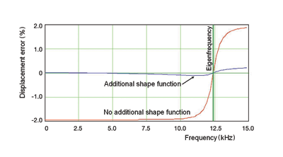
Additional shape functions can be added to improve the accuracy of a system simulation. Figure 1 shows an example of using modal superposition and additional shape functions to achieve a desired accuracy for package effects on a transducer [4].
Extracting modal shapes and frequencies from lab measurements is also easier than determining stiffnesses, so silicon validation of these models is straightforward. This highly accurate reduced-order modeling technique should be used for low-level verification of the component and system and must incorporate statistical modeling of the manufacturing distribution.

Fig. 1. Improved accuracy of reduced order models using modal superposition with additional shape functions [1].
Ideally, “point” or nonscalable model solutions should be avoided because they limit the ability of the designer to explore and optimize the design space at a system level. The model should parameterize the geometric, process, and environmental variables over both small- and large-signal behavior.
The transducer model is only truly useful if the component’s manufacturing distribution is accurately represented. Process variations, such as changes in film thickness and etch bias, lead to variations in transducer behavior that must be accommodated at the system level through signal processing. Underestimating this variability can lead to yield loss at final test, and overestimating it can lead to conservative designs that erode gross margin.
Once the core-model underlying equations accurately capture the impact of physical variables on transducer behavior, solid statistical models can be generated. Statistical distributions can be readily derived from manufacturing targets or a sampling of actual manufacturing data using techniques such as back-propagation of variance that are well known in the IC industry [5].
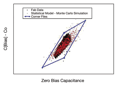
The advantage of deriving the statistics from metrics that are actually measured in the foundry is the ability to provide an ongoing method of verifying the alignment between the design environment and the manufacturing distribution. Figure 2 shows an example of comparing the silicon data to the statistical model for a given transducer test condition. The corner files encompass the statistical model results to a specific sigma level.

Fig. 2. The above is an example of comparing the silicon data to the statistical model for a given transducer test condition.
No matter which specific approach is used to build the transducer models, automation of the model generation is key to shortening the design cycle to the levels required to compete in today’s marketplace. To meet the product design demands of today and the future, commercial tools for MEMS system design must provide a means of taking results directly from the transducer designer’s finite-element environment and using them to generate compact transducer models that can be accessed by the system and circuit designers in an industry standard analog IC design flow. This method will improve cycle time, reduce errors, and allow for innovation in the design cycle.
MEMS models are used by the system and IC designer; therefore, the models should be integrated into the user’s design flow as tightly as possible. For the IC designer, this requires the model support all simulators and have multiple views for various levels of instantiation in the design flow.
Accomplishing this capability is no small task, requiring consideration of quality assurance, model verification, and best practices in library management. Model usage will suffer if an ad-hoc approach is practiced.
To facilitate a more structured model flow, companies should use design kits. These kits are analogous to standard IC design kits available from foundries and force the best practices mentioned.
Sensor companies should expect to augment any commercial tool available today and the foreseeable future. The tools and methods used in the MEMS design flow must address automated model generation, parameterization of variables relative to the system performance, scalable models, and IC design flow integration.
However, most notably investment is required to build solid statistical models that capture the manufacturing distribution and enable the ability to align the design environment to the manufacturing site over time. A MEMS flow that captures all the elements discussed is critical to achieving the optimal solution for next-generation sensor products. ■
References
[1] J. Mehner, L. Gabbay, and S. Senturia, “Computer-Aided Generation of Nonlinear Reduced-Order Dynamic Macromodels,” J. Microelectromech. Syst. , Vol. 9, pp. 269-278, 2000.
[2] M. Varghese, “Reduced-order modeling of MEMS us-ing modal basis function,” Ph.D Thesis, Massachusetts Institute of Technology (MIT), 2002.
[3] Q. Jing, T. Mukherjee, and G.K. Fedder, “Schematic-based lumped parameterized behavioral modeling for suspended MEMS,” Computer Aided Design , 2002. ICCAD 2002. IEEE/ACM International Conference on 10-14 Nov. 2002, pp. 367-373.
[4] J. Mehner, V.Kolchuzhin, I. Schmadlak, T. Hauck, G. Li, D. Lin, and T.F. Miller, “The influence of packaging technologies on the performance of inertial MEMS sensors,” Proc. of 15. Intern. Conf. on Solid State Sensors, Actuators and Microsystems , Transducers’09, pp. 1885-1888, Denver, 2009,
[5] Colin C. McAndrew, “Statistical Modeling for Circuit Simulation,” Proc. of Fourth Intern. Symp. On Quality Electronic Design (ISQED) ’03 .
Advertisement
Learn more about Freescale Semiconductor


