MEMS testing: innovations in mass production
The increasing penetration of MEMS into consumer applications presents continuous challenges to device testing
BY MARIO F. CORTESE and GIOVANNI AVENIA
STMicroelectronics
Milan, Italy
http://www.st.com/mems
This is the fourth in our series, Think Outside the Chip….MEMS-Based Systems Solutions. In previous articles, I and my fellow authors have addressed the basic concept of MEMS-based system solutions, the role of ASICs as interface circuits with MEMS devices, and co-design principles as they relate to the design interdependence of the MEMS/ASIC and package.
This article addresses the topic of MEMS testing. In a number of market research studies that I have conducted, it has been established that packaging, assembly, and testing can account for between 50-75% of the total cost of the solution with testing accounting from between 25% and 35% based upon the device and its intended application. Additionally, my research has established that many MEMS suppliers consider testing to be a major product differentiator in the market.
Efforts are underway to help the MEMS industry better understand the issues of MEMS testing and to develop testing standards for MEMS. In the Sensors Expo all-day session on June 7, 2010, as well the Microtech June 24, 2010, all-day sessions on MEMS-based systems solutions, presentations were made by individuals representing MEMUNITY on MEMS testing issues.
To quote their website, ”MEMUNITY is an open community of members from the MEMS manufacturing industry, research and academia. The goal of MEMUNITY is the development and promotion of wafer-level (and other) test techniques and equipment that enable the direct application of non-electrical input to each individual die, as well as the measurement of non-electrical output.” Although the focus of MEMUNITY has been on wafer-level testing, they address other aspects of MEMS testing. They have had frequent meetings (mostly in Europe) to discuss MEMS test issues and solutions. For more information, visit www.memunity.org.
With the recent commoditization of MEMS (example: accelerometers), the need to provide rigorous, high throughput and low cost testing is paramount in the battle for market share. After visiting ST Microelectronics’ facility near Milan, Italy, in March 2010, I was so impressed with the testing systems and strategies that they employ to test their multiaxis accelerometers, I invited them to contribute this article. I trust that it will inform and entertain you.
For more information on MEMS-based systems solutions, please plan to attend the MEMS Technology Summit on October 19 and 20, 2010, at Stanford University ( www.meptec.org/MEMSsummit/), as well as the MEMS Industry Group’s Executive Congress in Scottsdale, AZ, on November 3 to 5, 2010 ( www.memsindustrygroup.org) where I will be making presentations on MEMS-based systems solutions. I look forward to seeing you there.
Roger Grace
**************************************
Manufacturers of consumer MEMS devices face a number of key challenges to achieve a consistent and robust test platform for mass production. This article aims to sketch out scenarios for the testing of inertial and non-inertial MEMS in the years ahead.
The MEMS epiphany in consumer applications has brought about the challenge of how to test MEMS devices while at the same time guaranteeing high performance and cost efficiency. This challenge is continuously changing with the evolution of products, their performance, and complexity.
MEMS inertial sensors have been commercialized since the late 1980s in automotive applications, but their epiphany in the consumer market happened only in the first decade of the 21st century. The consumer market penetration has been possible only through the customization of existing MEMS test platforms and re-engineering of what had been already developed for the testing of standard semiconductor products. This gold rush has been driven in the past 10 years by the development of platforms capable of testing multiple MEMS devices at the same time with a physical stimulus, providing high levels of parallelism.
The challenge: moving it!
The first challenge with testing MEMS accelerometers is the need to apply the same level of acceleration the device will experience during its field life-time, both for low-g consumer applications as well as high-g applications in the Industrial/Automotive domain. Trials done by some MEMS manufacturers using electrical stimuli to avoid the application of physical stimuli during testing failed, due to the lack of correlation of product performances when the sensor is driven by electrical stimuli.
Applying physical stimuli to MEMS devices during testing guarantees the correct calibration of the devices, and keeps all the tolerances and parameter spreads related to front-end and back-end manufacturing processes under control. Parameters like zero-g level and sensitivity are fundamental for the final customer application and need to be guaranteed by proper calibration during testing on automated test equipment (ATE).
Customization of the existing semiconductor testing platforms (see Fig. 1 ), including the integration of the “moving” feature, has been done through:
• Creation, inside the handler structure, of a stimuli area (Rate Table) mechanically decoupled from standard handler movements, and
• Development of specific tools that avoid damage or mechanical stress to devices during testing or handling.
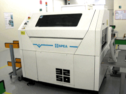
Fig. 1. Developed in cooperation with SPEA, this is one of the first ATE handlers used by STMicroelectronics for testing MEMS accelerometers.
A decoupled area in the handler that is insensible to stress/electrical noise/vibration is a must in MEMS accelerometer testers. This area generates only specific acceleration stimuli during the MEMS calibration/test phase without additional mechanical noise. The decoupled area requires a special electrical connection by cables going around the Rate Table in order to resist to mechanical stress generated from the constant and continuous application of acceleration and speed. The Rate Table structure must be also weighted in order to be insensible to vibrations.
Specific tools like pickers, as well as sockets, are also key to minimizing the mechanical stress on the MEMS devices during testing to avoid an incorrect calibration setup. The MEMS testing socket needs to ensure a very good clamping of the devices during the application of g-acceleration and a very low stress on the mechanical sensor inside the MEMS device. This has been achieved with the use of specific design and special polymer-grade plastics that allow the right level of performances and robustness across temperatures.
MEMS market explosion
The capacity to create equipment capable of handling high throughput has become one of the major challenges in sustaining the MEMS demand growth and key to success for MEMS manufacturers.
To increase the throughput, MEMS manufacturers need to:
• Increase the testing parallelism during calibration procedures (i.e., testing a consistent number of devices at a time), and
• Enhance electrical resources at the tester level to enable simultaneous measurements.
STMicroelectronics has devised a new-generation MEMS handler and tester (see Fig. 2 ) based on its previous experience with the MEMS Rate Table concept applied to the strip-testing format. This new platform allows testing to take place on a considerably high number of devices in parallel before the final package sawing.
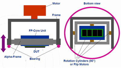
Fig. 2. The schematic (top) shows the flip-chip- bench functional format for MEMS testing platform (bottom). (Courtesy of MultiTest)
MEMS strip testing has presented the challenge of integrating a Rate Table inside a complex and high parallelism tool. ST found a solution with a new family of testing equipment that is capable of both handling high production volumes and generating for each single device constant and repeatable acceleration stimuli.
This revolutionary development has dramatically increased the total productivity per testing equipment. To achieve good performances in terms of a product’s main characteristics, some optimization was necessary. One of the main points was to minimize the residual stress on the MEMS device package. This has been achieved through a combination of the actions listed below, enabling a real revolution in terms of productivity in kpcs/day:
• The introduction of low-stress molding compounds,
• Customized pogo-pin connectors, and
• Dedicated conversion kits.
Although an alternative solution based on the Rate Table approach miniaturization was also developed and is currently available on the market, this new platform is widely used to calibrate devices for consumer market accelerometers.
What’s next and more…
Since 2008, the MEMS consumer inertial accelerometer has become “a must-have” in new-generation game consoles, smart phones, and several other consumer user-interface applications, such as remote controls. In the years ahead, the MEMS sensors will become part of our daily life in many other applications.
The MEMS technology has become mature, and new products like gyroscopes and inertial modules are arriving on the market. Integrating different sensors in one package, miniaturization, and performance improvements are the new challenges. Very soon it will be possible to integrate a complex-structure device — one that can sense not only acceleration, but also speed, pressure, magnetic field, and more — in the footprint-area of today’s MEMS accelerometer.
Success of these new products will depend on improved performance of handler platforms capable of guaranteeing throughput, flexibility and increased accuracy. This means equipment that will be able to generate different stimuli — magnetic, pressure, temperature, acoustics — and their combinations. A single testing platform capable of executing all these tasks will represent a new turnkey solution that will contribute to the decrease of the final product cost, catalyzing MEMS penetration in the consumer market.
Finally, miniaturization is the other trend that will drive the market in the second decade of MEMS consumerization. Smaller packages will fit into a much greater number of applications across many different fields, where dimensions currently are the limiting factor. MEMS testing equipment must be capable of handling very small devices without inducing mechanical stress or issues on the silicon.
Experience from traditional semiconductor fields is a good starting point for identifying a solution to this new challenge in the MEMS world. A good testing platform that guarantees a high level of flexibility regarding different stimuli and is capable of handling ever smaller packages is the key to success in the exploding MEMS arena.
The path is open, but there’s still a long way to go. ■
Advertisement
Learn more about Roger Grace AssociatesSTMicroelectronics


