MEMS: Think outside the chip… at the package level
Packaging is critical for today’s typical MEMS-based products, since it can be 20% to 40% of total material/assembly cost
BY ROGER H. GRACE
Roger Grace Associates, Naples, FL
www.rgrace.com
and
MARY ANN MAHER
SoftMEMS, Santa Clara, CA
www.softmems.com
The issue of MEMS-based system solutions and their packaging will be addressed at the MEMS Industry Group’s annual MEMS Executive Congress, which will be held in Scottsdale AZ on November 3-5, 2010, where Roger Grace will participate in a market panel discussion. For more information, visit www.memscongress.com. Also of note is the annual Smart Systems Integration Conference which will take place in Dresden, Germany from March 22 to 23. This event is sponsored by the European Technology Platform for Smart Systems Integration. Roger Grace is on the international steering committee of this event and will make a presentation featuring numerous applications of MEMS-based systems solutions. For more information, visit www.smart-systems-integration.org.
The packaging for a MEMS device is a critical component of delivering a successful MEMS-based system solution to the market. Our research has found that, for today’s typical MEMS-based products, cost of packaging can be 20% to 40% of the product’s total material and assembly cost. Since testing after packaging is much more costly than testing at the device level because of yield factors, it is crucial that the package be correctly selected/designed for the application.
Packaging strategies and tradeoffs must be considered and given significant attention by the design team from the very start, as well as throughout the entire design process. Many MEMS suppliers consider packaging to be a major product differentiator as well as a competitive advantage for their product in the market.
Package selection criteria
The design of MEMS packages are often more complex than the design of IC packages, as the former are frequently subject to additional design constraints and the requirement to operate in hostile media. The hostile media could manifest itself from the media to be measured. This could be as benign as dry air or as hostile as blood or radiator coolant. The other media is the environment in which the measurement is made. This includes shock, vibration, temperature, moisture, and EMI/RFI.
First, the MEMS package must interact with its environment. Examples include pressure inputs for pressure sensors and fluidic inlets for blood-processing devices. The MEMS package also must meet additional requirements on the mechanical and thermal budgets, as the output of the MEMS device may be a mechanical motion or a change in stress, so a package’s mechanical parasitics can interact and interfere with the functioning of the device.
For example, in a piezo-resistive pressure sensor, package stress affects the sensor’s output, as the various material compounds used in the package expand/contract at different rates, thus inducing stress on the sensor. In optical MEMS devices, package stress caused by shock, vibration, or thermal expansion may cause misalignment of optical devices and fiber interconnects. In the case of high-accuracy accelerometers and gyros, the package needs to be mechanically isolated from the MEMS chip to optimize performance (see Fig. 1 ).
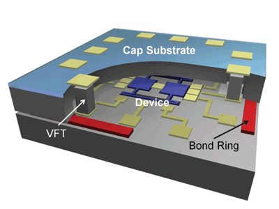
Fig. 1. Schematic of a generic wafer-level packaging (WLP) concept, showing a capping wafer simultaneously providing protection from the environment, via a bond seal ring, and interconnection using through-silicon vias (TSV). This arrangement allows autonomous integration of MEMS device and package. (Drawing courtesy of ePack)
As a result, MEMS packages may have stress compensation structures added to the package increasing cost and packaging complexity.
Depending on the type of MEMS device to be manufactured, the electrical performance considerations can dictate the type of packaging strategy employed. For example, capacitively sensed MEMS devices generate very small charges that must be sensed by electronics. Special care must be taken in the circuit design and packaging to maintain signal integrity.
Typically, most MEMS-based system solutions have associated electronic circuitry for compensation, control, and signal processing of the MEMS chip. Hence, a MEMS chip and a custom ASIC may be encapsulated within the same package. Alternatively, the circuitry may be monolithically integrated with the MEMS, requiring a single-chip package (see Fig. 2 ).
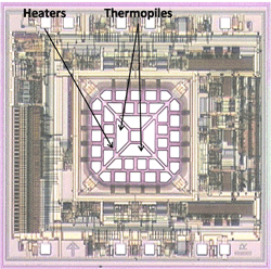
Fig. 2. This silicon monolithic thermally activated accelerometer includes a two-axis sensor, amplifier, A/D converter, heater control circuit, temperature compensation, and I2 C digital interface. (Photo courtesy of MEMSIC)
MEMS devices are also sometimes packaged at the wafer level; a capping process is used either to seal the MEMS to create a hermetic environment or to protect the moving MEMS devices before further packaging. This technique is often used for inertial devices such as gyros and accelerometers.
This packaging step is done in the MEMS fabrication facility in a clean environment using wafer handling. In contrast, for ICs most of the packaging steps occur at the chip level once the wafer has been diced, with lesser albeit still high restrictions on cleanliness.
MEMS designers would prefer to use standard packaging as much as possible to lower costs, and so adopt plastic packages or IC-compatible packaging whenever possible to take advantage of the IC industry’s cost structure. Using standard packaging also reduces design and test time, and the cost of the package itself is lower. A good rule of thumb is, if a MEMS device can be mounted on a PC board, it probably can be housed in a standard IC package (see Fig. 3 ).
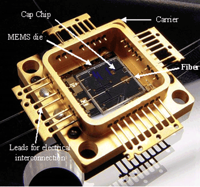
Fig. 3. The microoptomechanical system (MOEMS) switch die shown above is connected by four optical fibers and wire bonds and is housed in an industry standard Covar metal package. (Photo courtesy of University of Texas Arlington/ARRI)
However, many MEMS packages today are custom-made and optimized for the specific application since IC packages would not endure the punishment imposed by hostile media applications previously cited.
The challenges of MEMS packaging are further exacerbated especially in two application sectors: medical and automotive. In both applications the media to be measured is typically quite hostile to MEMS devices. In the case of automotive, engine oil, gasoline, radiator coolant, and exhaust gases need to be measured as to their pressure and chemical composition. In medical, blood, and urine are frequently measured media. Both share the need for high reliability and extreme ruggedness to achieve this end. Long life (especially with medical implantables), small size (see Fig. 4 ), and bio material compatibility (see Fig. 5 ) are significant issues to be addressed in the judicious selection of a package design and its materials and interfaces.
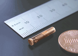
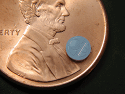
Fig. 4. This wireless, batteryless implant for monitoring cardiovascular hemodynamic pressure waveforms from ISSYS is a stand-alone, fully-functioning system, capable of telemetrically receiving power and transmitting pressure data. Its is 3.7 mm in diameter and 16 mm long, is hermetically sealed, and includes a MEMS pressure sensor (inset), an ASIC, and a communication coil. (Photos courtesy of ISSYS)
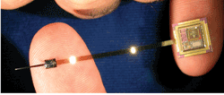
Fig. 5. This high-density cochlear implant microsystem uses a Silicon quartz paraylene packaging process, which provides bio compatibility, flexibility, and robustness for long-term operation. (Photos courtesy of the University of Michigan Wireless Integrated Microsystems [WIMS] Center)
Traditional MEMS packaging
MEMS were one of the early examples of SOC (system- on-chip) as integrated MEMS made in CMOS processes combined one or more MEMS devices, and analog and digital processing. MEMS products also make use of SIP (system-in -package) techniques integrating two or more chips in the same package as discussed previously. Wire-bonding was used to connect chips in a package for the first MEMS systems and currently this technique is being supplanted by flip chip bonding techniques taken from the IC industry (see Fig. 6 ).
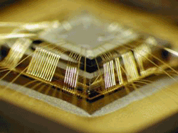
Fig. 6. In the chip-stack bonding of a silicon optical telecom switch device (bottom die) and CMOS control circuitry (top die), bond wires connect the top die to bottom die, as well as both die individually to the lead frame. (Photo courtesy of Aspen Technologies)
MEMS products also may be constructed from multiple wafers bonded together. This technique, often used in wafer-level packaging (WLP), is driven by the desire to use wafers of different materials, processed by different MEMS fabrication techniques. Currently, there is no market driver to standardize packaging (except when IC packages can be used), as companies see proprietary packaging technology as a competitive advantage.
Previously, designers often left design of packaging to the last moment after key sensor and circuit designs had been made. However, this trend is changing as time-to-market pressure and competition has forced designers to alter their design methodology as market windows were missed due to poorly functioning packages. Lack of design tools has caused package over-designs or package failures, as stress and other effects were not properly estimated. New tools for co-design of package, electronics, and MEMS devices are enabling better package designs. (See “Electronics for MEMS: design issues and tradeoffs,” www2.electronicproducts.com/E-article-farc_grace_apr2010-html.aspx)
New developments
New techniques for packaging have come out of advances in MEMS device fabrication. Through silicon-vias (TSV) are the results of techniques for etching all the way through a wafer for a depth of up to 100s of microns . As a result, MEMS wafer fabs are supplying this important packaging step as well as creating the MEMS devices.
TSVs enable another important packaging technique- that of chip stacking whereby multiple chips are stacked together inside a package and connected together with TSVs. Chip stacking creates a smaller packaging footprint. The design of such a package is more complex as there are thermal dissipation issues as heat must be removed between the chips stacked in close proximity and the mechanical stability must be carefully simulated to ensure good performance and reliability. Traditional IC packaging houses are also beginning to offer MEMS-specific packages and equipment vendors are jumping in to supply new packaging and testing equipment. Hence, the packaging options for MEMS devices are numerous and the trend of MEMS incorporating multiple sensors along with associated software to create higher added value systems is converging with the availability of new multichip packaging solutions. Chip stacking can be realized in a one-at-a-time fashion or through wafer level packaging (WLP) approach addressed earlier.
Future directions
One important new direction in packaging is to use flexible substrates to package together rigid components. Multiple sensors can be combined with electronics and power modules. By folding, the packaged system can fit in a small form factor. This technique is especially attractive for wearable body sensors (see Fig. 7 ).

Fig. 7. Multilayered assemblies of rigid components on flexible substrates allow integration of multiple sensors onto a single, small, lightweight autonomous wireless node. The foldable configuration reduces space. (Photos and drawings courtesy of Bozena Kaminska)
Standardizing packages will most likely occur as companies focus on other value-add as was done in the IC industry, but this trend will take time. Where and by whom packaging is done will also evolve over time as MEMS and semiconductor fabs and traditional packaging houses compete to supply the newest and highest-performance packages and as more traditional semiconductor foundries offer services to the MEMS community.
It is noteworthy that through-substrate vias started with the development of the silicon capacitive pressure sensors product at Ford in the early 80’s using laser drilling of glass. Thirty years later, we anticipate that this MEMS-based packaging techniques will not only have a huge impact on the MEMS industry, but also on the IC industry, where it is estimated that in the not-too-distant future more MEMS wafers will be used for IC device packaging than for MEMS products. ■
Advertisement
Learn more about Roger Grace AssociatesSoftMEMS


