Designers have many questions to answer before choosing the right NAND flash memory for their applications
BY SCOTT NELSON
Toshiba America Electronic Components
Irvine, CA
http://www.toshiba.com/taec
In the past few years, NAND flash has become the storage solution of choice for a wider and wider range of applications, spurred by a steadily decreasing price/bit achieved by advances in multi-level cell (MLC) technology and progression to smaller process geometries. NAND flash has enabled multiple markets and today is gaining ground in laptop computers both in solid state drives and various cache solutions.
Questions with fuzzy answers
This proliferation of NAND flash, however, brought additional questions for system designers to consider. When is it best to use MLC NAND vs. SLC (single level cell) NAND? What exactly does that choice mean in terms of power, speed, error correction requirements, and usable life?
The answers to these questions are not as straightforward as one might expect, because of the rapid progression of NAND flash from one geometry to the next, and a proliferation of NAND manufacturers, each using slightly different process geometries. For each process node, such as 56 or 43 nm, the specifications for MLC vs. SLC NAND performance is different.
For those not familiar with the technology, MLC NAND flash allows each memory cell to store two or more bits of information, compared to one bit per cell for SLC NAND (see Fig. 1 ). MLC NAND has a larger capacity, lower bit cost, and a decrease in several performance parameters. However, for many applications, MLC NAND provides more than suitable performance and longevity, and has helped make storage more affordable. When given a choice, such as with high-performance memory cards or USB drives, most customers have not been willing to pay for the additional performance available from SLC NAND.
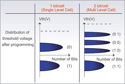
Fig. 1. MLC NAND uses four threshold voltage levels within a cell to be able to store two bits of data per cell, compared to two voltage levels and one bit per cell for SLC NAND.
SLC NAND is typically used today for selected applications that require either higher speed or greater endurance to justify its price premium. According to market analyst firm Web-Feet Research, MLC NAND shipments were approximately 78% of total NAND shipments in 2007. The important thing is to choose the appropriate performance level for the specific application to balance the value/performance equation.
Design tradeoffs
For any specific process geometry, MLC NAND writes data at approximately one half to one third the speed of SLC NAND, requires a higher level of error correction, and has lower write cycle endurance.
Power . The basic circuitry for MLC and SLC chips is similar, and power consumption for the two types of memory is approximately the same.
Speed. As noted above, SLC and MLC NAND specifications change with each process geometry, and can vary by manufacturer. As a rule of thumb, SLC NAND is generally two to three times faster than MLC NAND. Toshiba MLC NAND with a 4 Kbyte page size has a write speed of 4.5 Mbytes/s using single plane capability, or 9 Mbytes/s in dual plane. The write speed for the comparable SLC device is approximately three times faster.
Error correction. Just as hard-disk drives have some bad sectors, NAND works in a similar way in that the controller maps around bad memory areas and error correction (ECC) is used to correct bit errors. The industry standard is to correct any bit error to a level comparable to that of hard-disk drives, or 1 x 10-14 , which means one bit uncorrectable error every 1014 bits (12.5 Tbytes). For any given process node, MLC NAND requires a higher level of ECC than SLC NAND to achieve this level of error correction.
The industry provides embedded NAND solutions with dedicated memory controllers optimized to provide ECC, wear leveling and other NAND management capabilities (see Fig. 2 ) so designers do not need to implement ECC themselves, or be concerned about the difference between ECC requirements for MLC vs. SLC NAND.
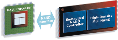
Fig. 2. The industry has moved to self-contained embedded NAND solutions with dedicated controllers to handle ECC, wear-leveling, and other management functions.
Endurance. MLC flash has a different rating for the number of write/erase cycles compared to SLC NAND flash. Today, most SLC NAND flash is rated to have approximately 100,000 cycles, while industry specifications for MLC range from 3,000 to 10,000. While that sounds like a huge difference, specific application usage models are easier to understand and evaluate.
As an example, based on our usage modeling, MLC-based solid-state drives (SSDs) are a good fit for most mobile computing applications, while SLC-based SSDs are better suited for high-performance enterprise applications.
Absent any industry-standard usage model for NAND-based solid-state drives, Toshiba developed an internal model and studied usage patterns for typical and heavy mobile computer users. Typical users wrote approximately 1.4 Gbytes/day, and heavy users about 5.2 Gbytes/day.
To even begin to reach a conservative endurance limit of a 64-Gbyte MLC NAND-based SSD with wear-leveling technology, a mobile user would have to write approximately 40 Tbytes of data over the expected five-year life of the drive. That’s equal to approximately 22 Gbytes of new data per day, every day.
With a 128-Gbyte drive, the wear would be spread over a larger storage area, doubling the average daily limit to 44 Gbytes. Therefore the endurance limit is so far beyond the likely usage of a typical mobile computer user that it may not be a realistic cause for concern.
On the other hand, applications that involve nearly constant writing might require SLC NAND. Examples may include an enterprise solid state drive, or a personal video recorder (PVR) that constantly records an hour of video, then rewrites the previous hour’s images to record the most recent video stream.
For example, a 4-Gbyte PVR, recording video at a rate of 1 Mbyte/s, would write a total of 86.4 Gbytes/day, and would use one complete write cycle every 1.1 hours. In this example, the 100,000 rated write cycles of SLC NAND would last approximately 12 years, more than enough to meet the typical 5-year product life, while MLC NAND rated at 10,000 cycles would last only 1.2 years. ■
For more on NAND flash memory, visit http://www2.electronicproducts.com/DigitalICs.aspx.
Advertisement
Learn more about Toshiba America Electronic Components


