BY DIMITRY GODER, Director of Product Definition;
KEN SALVI, Business Manager;
NAZZARENO ROSSETTI, Ph.D. EE
Maxim Integrated
www.maximintegrated.com
In the long electric path from the power source — be it the AC line or the battery — to an electronic load, the low-dropout (LDO) regulator is often called upon to cover the “last mile.” Here, the noisy switching regulator steps aside in favor of the quiet LDO to power critical electronic loads. The LDO has been under constant renewal or evolution along with the rest of power management electronics. Over time, the LDO has not only become quieter but more reliable, accurate, fault-tolerant, powerful, and efficient, with a mix of features that adapt to the application at hand.
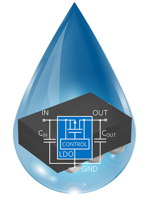
Fig. 1. State-of-the-art low-dropout regulator: smaller than a drop of water.
Recent applications like miniature wireless 4G base stations have challenged the already small LDO to become even smaller while packing more power. In this article, we’ll review the main features of an LDO while comparing a modern CMOS LDO to an old bipolar workhorse. Subsequently, we’ll review how each LDO parameter helps solve a specific application problem. We’ll then introduce a new family of LDOs with features that enable further miniaturization, enhance fault tolerance, and support a broad range of modern applications.
LDOs have come a long way
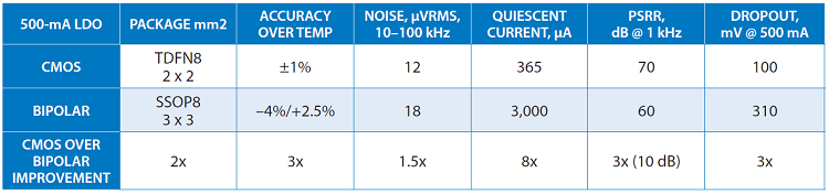
Table 1 compares the main features of a pioneering bipolar LDO regulator with an integrated PNP pass transistor (2.1- to 16-V input voltage) to a modern CMOS LDO with an integrated PMOS pass transistor (1.7- to 5.5-V input). As you can see from across all of the features listed, the CMOS LDO outperforms the old bipolar one by a factor ranging from 1.5 to 8 times!
Table 1: Bipolar vs. CMOS LDO regulator comparison.
The following LDO parameters are important for the application at hand:
Low noise and high PSRR. In wired and wireless communication systems, the LDO provides a clean power supply to sensitive analog circuits (PLL, VCO, RF). The LDO must have good power-supply rejection ratio (PSRR) to isolate its load from its source, likely due to a noisy switching regulator. Low spectral noise (VRMS /√Hz) will minimize linearity degradation in the RF demodulator and phase noise in the PLL and VCO circuits.
Low quiescent current. In operation, the quiescent current of an LDO will dissipate additional power. A 4-mA quiescent current with a 5-V input (as shown for the bipolar LDO in Table 1 ) will dissipate 20 mW. This robs the regulator of almost another whole percentage point of efficiency. The CMOS regulator, with only 365 µA of quiescent current, can reduce this loss tenfold. This is significant because low quiescent current is as important as low dropout in portable applications.
High output accuracy. Additional power dissipation can occur due to an output voltage that is higher than nominal, even when within an acceptable range of tolerance. At 4% accuracy over 5 V and 500 mA, you will see a power dissipation increase of 4% x 5 V x 500 mA = 100 mW. This is as costly as the losses from the pass transistor of the previous case! This is inadequate for power-hungry portable applications.
Low leakage. Even while not in operation, the LDO needs to perform efficiently. Wearable devices are typically very small in size and must last a long time both in operation and on the shelf. Minimization of the size and power dissipation in both modes is crucial. While on the shelf in shutdown mode, the device might need to last up to three years, which requires a very low leakage current.
New requirement: reverse-current protection. Reverse-current protection is a new feature seldom found in available LDOs. In battery-operated equipment, the load is regulated typically via an efficient CMOS LDO with a MOSFET pass transistor that carries a reverse-biased intrinsic diode between input and output.
The reverse-current protection prevents the large reverse current that occurs when a buck regulator at the LDO input is shut off, shorting the input to GND. The discharge energy of a large LDO output capacitance through the LDO pass transistor’s intrinsic diode creates the damage. A low reverse current is tolerated. Above a set threshold (200 mA), the reverse current is completely blocked.
New requirement: Miniaturization. As seen in Table 1 , little progress has been made in LDO packaging miniaturization. This is due, in part, to reliability concerns. In harsh environments like automotive under-the-hood applications, lead-frame IC packages like the TDFN-8 are preferred because they have proven their high reliability over time. Lead-frame technology is inherently space-inefficient.
On the other hand, in consumer and wireless communications applications, size is a major concern. Fortunately, these environments are relatively benign and stress-free, opening opportunities for innovation.
Can we preserve all of the progress made by LDO electrical parameters and add additional features like fault tolerance with reverse-current protection and miniaturization for wireless applications? A new family of LDOs positively answers this challenge.
A state-of-the-art solution
The excellent parameters shown in Table 1 for the CMOS LDO are applicable for the MAX38902A/ MAX38902B/MAX38902C/MAX38902D family of LDO regulators. Going even further, this new family solves the miniaturization problem by providing an option of wafer-scale packaging technology, resulting in minimal PCB space usage. In addition, it solves the reverse-current protection problem with a novel implementation of the LDO power train. Let’s review these innovations in more detail:
Wafer-scale packaging. Miniature 4G base stations are small enough to fit in a backpack and are still very powerful. Here, the LDO that powers the RF section must be small and powerful, delivering hundreds of milliamperes. The C and D versions of this newer LDO family adopt wafer-level packaging (WLP) technology for increased miniaturization. Fig. 2 illustrates how the 500-mA LDO regulator, in a WLP-6 package, occupies roughly one-fourth the space of the TDFN-8 footprint (and one-sixteenth of the SOT23-5 of Fig. 4 ). The WLP-6 solution is well-suited for applications that require minimal PCB space.
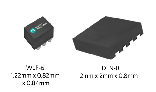
Fig. 2: MAX38902C/D WLP-6 package advantage.
Reverse-current protection. The pass element (T1 in Fig. 3 ) is a low RDSON p-channel MOSFET transistor. The internal circuitry senses the MOSFET drain-to-source voltage and, in addition to driving the gate, keeps the body diode reverse-biased. This additional step allows the device to behave like a true open switch when its polarity is reversed (LDO OUT 10 mV higher than LDO IN). A positive drain-to-source voltage, under proper drive (CONTROL), turns the MOSFET “on,” with current flowing in normal mode while the body diode is again reverse-biased.
This innovative feature protects the load and the LDO from accidental input shorts, making the system more fault-tolerant.
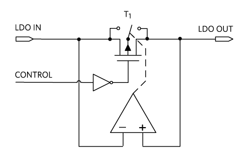
Fig. 3: MAX38902A/B/C/D reverse-voltage protection.
High-reliability applications. Industrial and automotive applications are characterized by a wide operating temperature range. Here, a lead-frame package, more tolerant of temperature-induced PCB surface mechanical stress, may be preferred. In this case, a modern TDFN package (A and B versions) provides a solution that is roughly half the footprint and two-thirds the height of a more traditional SOT23-5 or similar package (Fig. 4 ).
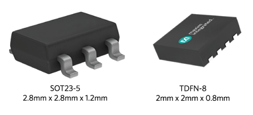
Fig. 4: MAX38902A/B TDFN-8 package advantage.
Low noise performance. Fig. 5 shows the spectral noise density of this family of devices. With a figure of merit as low as 30 nV/√Hz), it is an excellent choice for many low-noise applications.
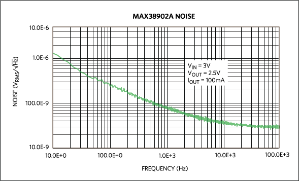
Fig. 5: MAX38902A/B noise performance.
High PSRR performance. Fig. 6 shows the PSRR profile from 100 Hz to 10 MHz. With a figure of merit as high as 62 dB, this family is an excellent choice for analog or digital noise-sensitive applications.
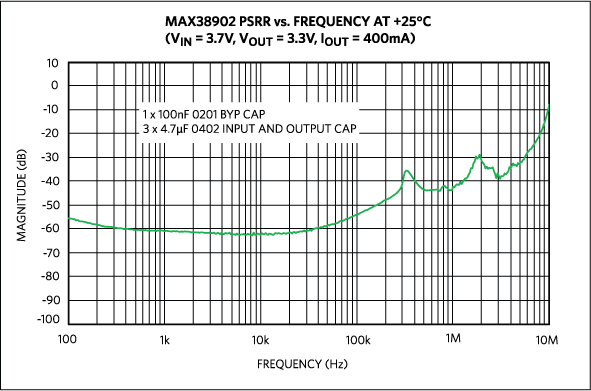
Fig. 6: MAX38902A/B PSRR.
Conclusion
LDOs have come a long way since their initial introduction by adapting to the needs of evolving applications. We reviewed the classic LDO parameters and discussed its improvements moving from a bipolar to CMOS implementation. Next, we discussed the challenges of reverse-current protection and the miniaturization required by many modern portable applications. A new family of LDOs (MAX38902A/B/C/D) solves the former problem with a new power train architecture and the latter problem with the adoption of wafer-level packaging options. For challenging application environments such as industrial and automotive applications, traditional lead-frame package technology is also available.
The availability of multiple versions of the basic LDO supports different applications. This gives system designers several “go-to” LDOs that can be leveraged to save significant cost and development time.
Advertisement
Learn more about Maxim Integrated


