By Patrick Mannion, contributing editor
What were once coprocessors are now becoming the processors as designers make parallel data processing a central element of heterogeneous architectures for artificial intelligence (AI), natural language processing, and image processing.
To be sure, CPUs from Intel, AMD, Arm, and the open-source RISC-V architecture will still play a role in control-plane processing and even signal-processing functions where appropriate. However, the emphasis is clearly shifting to arrays of multiply-accumulate (MAC) functions optimized for the fast and efficient execution of deep neural network (DNN) and convolutional neural network (CNN) algorithms.
DNN is mostly used for AI and natural language processing. A simple example is the Echo Dot from Amazon, a seemingly simple front-end device that is supported by massively parallel AI and natural language processing farms. CNN is increasingly being used for computer vision processing, with particular interest in efficient CNN solutions coming from automobile manufacturers looking to further augment their advanced driver assistance systems (ADAS).
For designers of data centers and edge-based systems looking to take advantage of DNN and CNN techniques, classic architectures are playing second fiddle to massive GPUs from Nvidia and power-sipping CNN processors from videantis GmbH.
For example, Nvidia’s latest Tesla V100 GPU accelerator uses the Volta GV100 GPU, which continues to set the standard in the data center (Fig. 1 ). The GV100 is based on the company’s Pascal GPU, packing 21.1 billion transistors into a die measuring 815 mm2 and using TSMC’s 12-nm FinFET Nvidia (FFN) manufacturing process. The GV100 version further simplifies programming and application porting and improves GPU resource utilization.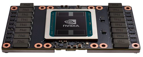 Fig. 1: Nvidia’s Tesla V100 accelerator is based on its GV100 GPU, which continues to set the standard for high-performance data center, AI, and deep-learning systems and applications.
The Volta iteration has a redesigned Streaming Multiprocessor (SM) architecture and is 50% more efficient than the Pascal design. The new Tensor Cores, specifically designed from deep learning, provide up to 12x higher peak teraflops for training and 6x higher peak teraflops for inference. Other features include support for six second-generation Nvidia NVLinks, with a total bandwidth of 300 Gbytes/s, 16 Gbytes of HBM2 memory, and optimized software for deep-learning frameworks such as Caffe2, MXNet, CNTK, and TensorFlow.
TensorFlow is Google’s deep-learning framework, and the company backs it up with the Tensor Processing Unit (TPU) (Fig. 2 ). Google designed the TPU ASIC as an alternative to current GPU and CPU architectures to perform neural network processing at scale for applications such as Google search, Google image processing, and Google Translate.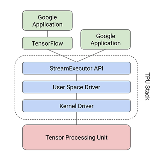 Fig. 2: Google’s TPU was designed to perform neural network computations at scale for Google search, Google image processing, and Google Translate.
The TPU was implemented in a 28-nm process, runs at 700 MHz, and consumes 40 W. As Google needed to deploy it quickly to meet the needs of data centers that were quickly reaching their limits, it comes as an accelerator card that fits into a SATA slot. It connects to the host over a PCIe Gen3 x16 bus. This interface has a bandwidth of 12.5 Gbytes/s.
The TPU is a leap forward in performance relative to CPUs and GPUs. At the heart of the processor’s performance capability is the Multiplier Matrix Unit (MXU) arranged in a systolic array. While general-purpose CPUs are sequential with a read-operate-write process, the MXU’s systolic array means that it can read an input value and perform multiple operations on it without storing it to a register. It’s called systolic because data flows through the chip’s array in waves, like how a heart pumps blood.
The MXU approach is optimized for power and area efficiency and can perform 65,536 MACs for 8-bit integers every cycle. As it runs at 700 MHz, that means that it can perform 46 x 1012 MACs/second. This compares favorably to a RISC CPU in the context of DNNs, as they typically can only perform one or two arithmetic operations per instruction. GPUs can execute thousands per second.
Google’s TPU and Nvidia’s Tesla V100 are at the head of a flotilla of alternative processing architectures, with AMD and Intel playing catchup. That said, Intel has acquisitions such as Nervana and Altera that have yet to be fully leveraged, while Microsoft has demonstrated its Brainwave software running on Stratix 10 FPGAs achieving 39.5 teraops/s. It expects to achieve 90 teraops/s on production silicon running at 500 MHz.
Bringing CNN to the edge for vision
As new and established silicon and software providers jockey for DNN positioning at the data center, videantis GmbH announced a CNN vision processor and development tool chain aimed squarely at the edge. In particular, the v-MP6000UDX visual processing architecture and v-CNNDesigner tool target smart image and video processing (Fig. 3 ).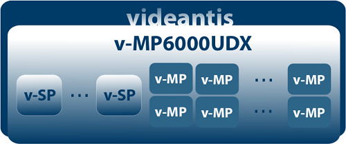 Fig. 3: The videantis v-MP6000UDX combined with the v-CNNDesigner tool accelerates development of smart image sensors at the network edge.
According to Marco Jacobs, vice president of marketing at videantis, CPUs and GPUs by themselves are not efficient enough for image sensing and processing at the edge, so it developed a digital signal processor in 2004 for low-power applications. The 6000 series is its latest instantiation, this one intended for DNN and CNN algorithms.
Unlike the TPU, it’s not also intended for training. Instead, said Jacobs, once the training is done, a designer can take the developed code, run it through v-CNNDesigner, and map that code to the v-MP6000UDX cores in minutes. Training is the process of identifying objects such as different animals, road signs, pedestrians, and other objects in different situations and against varying backgrounds. The process is labor-intensive, can take weeks, and results in several megabytes of final code. However, once generated, the code is run through v-CNNDesigner to greatly simplify the transfer and mapping process. The v-MP6000UDX processor itself operates at 50 teraops/s, said Jacobs, with the efficiency depending on the process node and other implementation factors.
Smart sensing devices, ADAS, and smartphones are obvious target applications, along with drones, self-driving cars, virtual and augmented reality, and surveillance. What videantis is doing is just the beginning of a very interesting time for computer vision, thanks to advances in neural network processing. “In 2012, there was a big CNN breakthrough,” he said, referring to AlexNet, a CNN that competed in the ImageNet Large Scale Visual Recognition Challenge that year. “Now the second trend [data centers were the first] is to make them smaller and more power-efficient so they can run on embedded devices.”
With CNN innovations occurring daily, Jacobs emphasized that the v-MP6000UDX runs a variety of algorithms, making it future-proof. For now.
Advertisement
Learn more about Electronic Products Magazine


