BY DAVE ANDERSON
CEO
Novati Technologies
www.novati-tech.com
A relative newcomer on the industry’s radar, and initially overlooked for the utilization of exotic materials, More-than-Moore (MTM) technologies have brought rapid changes for microelectronics performance and reduction in power consumption. For instance, reflecting a huge benefit gained from new materials and engineering approaches, the pace of development for today’s devices, systems and methods has improved by double. These improvements promise a significant advantage for integration of heterogeneous components and enabling the Internet of Things (IoT).
Introducing MTM
MTM technologies broadly expand the landscape for creating novel systems without the burden of relying on the very smallest nodes. This advancement includes the vertical integration of MEMS, various III-V substrates, and silicon onto a single chip. Equally valuable is the ability to complete the stacking and production without sacrificing yield.
As the first track to be launched for the global chip industry since publication of the original International Technology Roadmap for Semiconductors (ITRS) in 1998, MTM is expected to address the exploding demand for products that don’t require bleeding-edge scaling. When the roadmap was created, a modest few hundred companies and universities contributed to the vision for milestones that would ensure a concerted direction for the world’s microelectronics ecosystem.
Today, nearly 1,000 organizations from industry, academia, and government connect to provide guidance for ITRS to help ensure progress for the industry and its customers. Many of those same players also are collectively helping to steer creation of the new ITRS extension, an MTM roadmap.
From a global perspective, the MTM revolution aims to extend the use of the silicon-based technology developed in the microelectronics industry to provide new, non-digital functionalities. This approach for enabling new technologies mirrors the resources built up for decades to drive the multi-billion-dollar semiconductor business. Regarded in the past as too exotic because of concerns about costs and contamination, thousands of new combinations of elements are now being used to produce state-of-the-art components.
To exploit this new pool of technology, nanoelectronics communities are presented with an exponentially greater number of resources that provide a significant advantage over traditional silicon foundry offerings. For example, Novati Technologies’ development center utilizes more than 60 elements from the periodic table (Fig.1 ). By contrast, traditional foundries worldwide have limited their customers to less than 25 of those elements. The sharply expanded diversity and supporting expertise at the new, smaller nanofabrication center enables a broader range of capabilities to fabricate unique MTM devices on existing CMOS platforms.
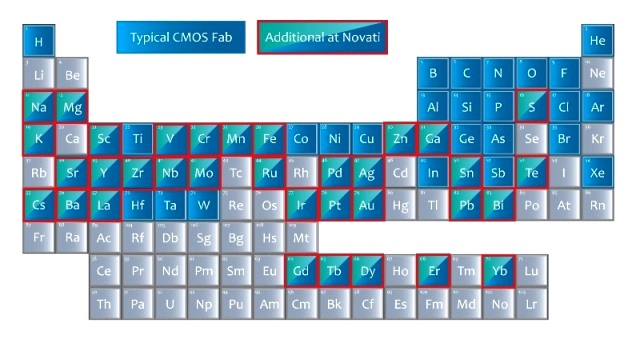
Fig. 1: More-than-Moore technologies involves mastery of a greater number of elements for use in device foundries. Novati has more than doubled the number of elements traditionally used in foundries, adding 34 to the traditional 25. Use of these additional elements result in materials and devices with previously unseen properties.
A “Moore” perfect union
The growth in the number of desired materials and the ability to merge MEMS and CMOS together has become a celebrated combination. On integrated MTM devices, the MEMS devices can leverage the aggressive scaling of modern CMOS. Not without some hurdles, one challenge to consider in their integration is to ensure that the intended functionality is not compromised in the conjunction.
Advantages of this union include better fidelity as the signal to noise is improved through the massive reduction of parasitics. This also manifests as improved measurement bandwidth–increasing the rate at which measurements can be taken. When compared with discrete MTM and CMOS devices on separate chips that interact on a board, this direct interconnectivity of integrated devices results in a massive reduction in power usage and overall board space. Combining these positive attributes, reduced parasitic interference contributes significantly to an improved Q Factor and faster cycle times.
Further, although sensors have been around for decades, novel sensor designs are now made possible through the direct integration of MEMS devices on top of silicon or bonding different die on top of each other (3D integration). The potential is limitless for the previously unimagined combinations to drive comprehensive changes and progress for the microelectronics industry.
Elegant integration without yield loss
With the benefit of proven tools and methodologies–continuously refined by industry for decades–we can employ low-risk processes for high-yield results. For instance, by needing only one package and die cut, companies gain a lower cost of die. To ensure yield, the CMOS is tested prior to the integrative steps with MEMS and sensors.
By placing devices together rather than individually apart, the conservation of source materials gained from integration improves the ROI. This has influenced the ability to adopt new high-k materials and other compounds like indium-arsenide and niobium-titanium that enable significant progress across a wide range of commercial and security markets.
A critical part of this equation for reliable yield of novel materials is a fabrication facility that is “CMOS clean.” New materials are introduced and monitored to maintain CMOS cleanliness standards for shared processing tools. A rigorous approach to quantify and remediate trace metal contamination is followed for all tools exposed to new materials, thoroughly minimizing risk of cross contamination.
With the break from past limitations and a receptive fab, MTM-class nanofabs can safely engage an unprecedented number of elements in order to move innovative ideas and breakthrough designs into production. Novati is an example of the new type of nanofab that is the first to offer this level of expanded product development capability, along with the few others who can quickly upgrade to support this emerging direction.
This more sophisticated level of device integration provides the convergence of improved performance, power consumption and functionality that enables rapid advancements for markets that include consumer, healthcare, transportation and manufacturing.
In their exploitation of newly combined building blocks, companies and organizations must consider that manufacturability continues to be a key technical risk-factor for MTM technologies. Providing affordable manufacturability of breakthrough technologies requires a significant investment across a range of capabilities.
Beyond electrical and industrial engineers, these novel MTM technologies demand significant expertise from chemical engineers, mechanical engineers, device physicists and equipment specialists to produce desired results. Investment in robust quality systems is also crucial, helping to manage the risks inherent with incorporating a larger material set.
To demonstrate their new innovations, designers must fabricate complete cells, which require re-development and optimization of a number of standard process steps, unrelated to the product. The new generation of nanofabs aims to reduce start-up time and provide access to a shared manufacturing knowledge base and capabilities. This progress means not having to reconstruct standard technologies–previously a big challenge for both commercial and government interests. By leveraging these advantages, customers of MTM nanofabs are able to nearly halve their development time and number of learning cycles.
As a result of these many improvements for device development, large corporations, small startup ventures, university spin-offs and defense contractors that have influenced creation of this strategic nanofabrication model will exploit designs and advantages that more traditional venues are simply not able to offer.
Setting a new standard
As the solution for affordable convergence, MTM is fast becoming the de facto solution for commercial and security applications. By extension, component integration will accelerate the systems integration envisioned by the Internet of Things. And there’s a lot at stake. As an indication of the market to be seized, more than 85% of things are not yet “connected” today.
The rapidly growing set of novel and extended methods for connecting the IoT heralds that MTM is the key to a future where nanofabrication facilities with fresh combinations of elements will accelerate the integration of so many more things. The opportunity is massive for the communities that drive an enhanced quality of life for the planet.
Assessing this convergence, analysts predict that by 2020 as many as 75 billion connected devices will depend on state-of-the-art MEMS, advanced sensors and other key factors like the 2.5 and 3D technologies that will enable integration for novel materials.
As a result of this aggressive innovation, the era for enabling the most rapid, and affordable, product development and deployment has begun. And the chip industry gains new ways to rival the growth of its past.
Advertisement
Learn more about Electronic Products Magazine


