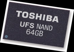
Electronic Products’ Technical Editor Jim Harrison explores some frequently asked questions regarding the future of embedded memory for consumer electronics.

Q: What is special about UFS flash memory devices?
A: Universal Flash Storage (UFS) uses a very fast serial interface and is based on a JEDEC standard (in 2011). UFS chips have a built-in flash controller, like e-MMC. UFS uses MIPI M-PHY and MIPI UniPro interfaces and is said to be faster and more energy efficient than the current e-MMC interface. Initial versions of UFS devices (Ver1.1) have been sampling in the market since early 2013 to enable chipset and OS development for this new standard. The large photo and video data files being moved around from smartphone and tablet computers are driving the industry to find faster, more secure transfer mechanisms.
Q: Are there advantages that UFS holds over the e-MMC memory interface?
A: The increasing demand for fast data transfers in phone and tablet platforms will favor rising usage of UFS over the next couple years.
I talked with Scott Beekman, Director, Managed NAND Memory Products and he noted, “UFS not only provides a faster interface relative to e-MMC, it also enhances overall system performance with capabilities such as full duplexing, enabling both reading and writing between the host system and UFS device at the same time. Toshiba was the first to introduce embedded devices supporting the UFS interface and has been sampling since early 2013. Going forward, we will continue to maintain a leadership position in UFS solutions.”
So, UFS Ver2.0 has data transfer speeds of up to 2.9 Gbits/s per lane, and multi-lane configurations can be supported. With two lanes we have 5.8 Gbits/s — almost double the maximum interface that can be supported against the latest e-MMC standard Ver 5.0, which can support DDR 200 MHz with eight I/O (3.2 Gbits/s). UFS uses the SCSI command set and architecture model, and has a roadmap for even faster transfer speeds in the not-too-distant future.
The UFS device supports multiple commands with command-queuing features and enables a multithreaded programming paradigm. This differs from e-MMC and other embedded flash solutions, which process one command at a time — limiting random read/write access performance.
Q: Will UFS soon replace e-MMC?
A: Initially, UFS parts will be higher priced than e-MMC, and early on will likely be adopted by higher-end applications, that need enhanced performance, before migrating to mid- and lower-tier products in the future as the price gap decreases. For this reason, e-MMC is expected to remain in the market for some time in parallel with UFS.
Q: I know Toshiba has been sampling a UFS flash memory. When will there be general availability?
A: The UFS system has the backing of Toshiba, Micron Technology, Nokia, Samsung, Sony Ericsson, Spansion, STMicroelectronics, and Texas Instruments. Toshiba has been sampling the UFS Ver1.1 64-Gbyte devices, THGLF0G9B8JBAIE, since January. These devices come in a 169-ball 12 x 16 x 1.2-mm FBGA package. More UFS devices are expected to be introduced later this year, and mass production for UFS is expected to ramp more broadly in the market in early 2014.
Advertisement
Learn more about Toshiba America Electronic Components


