BY SYLVAIN DUBOIS
Senior Director
Strategic Marketing and Business Development
Crossbar, www.crossbar-inc.com
The first wave of digital data growth is coming from user-generated content made up of images and videos recorded by mobile devices and uploaded almost instantly onto social networks. The rise of cloud-based media storage services for private or shared usage has removed the limitation of electronic device storage capabilities. The frontier is limited only by the available capacity of cloud storage providers.
As the Internet of Things (IoT) continues to gain momentum, digital data stores will be fed by billions of connected and smart devices. Sensors are acquiring information which is being processed by ultra-low power MCUs and uploaded via low-power wireless communication protocols and the Internet in an extremely integrated and cost-efficient manner. An IDC report published in Dec. 2012 projected that the digital data universe will reach 40 zettabytes (ZB) in 2020, a 50-fold growth over a 10-year period. This exponential increase requires massive investments in enterprise IT infrastructures and innovative solutions in hardware and software.
The challenges of technology scaling
Moore’s Law has been the guiding rule of the semiconductor industry for almost half of a century, and the steady growth of transistor density enabled improved processing capabilities. The memory industry wasn’t able to keep pace and memory and storage became the performance bottleneck of advanced architectures.
Flash technology is based on storing and measuring numbers of electrons in the gate of a MOS transistor. At each new technology process node, the transistor and memory cell shrinks, resulting in fewer electrons. In today’s current technology process nodes, there are barely enough electrons to maintain a sufficient charge sensing level to meet performance and reliability requirements.
To work around these limitations, complex algorithms have been integrated into memory controllers. In the nanoscale of flash technology, there are an increasing number of failed bits that require to be corrected to avoid missing pixels or, worse, missing a byte of code. The implementation of such sophisticated logic requires fast computing logic and DRAM buffering that introduce latencies and additional power consumption. Flash-based technology may have hit its scaling limit, while the demand for storage continues to grow exponentially.
Resistive RAM
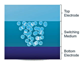
Resistive RAM technology is based on the motion of discrete nano-particules under the influence of an electric field or heat, and the ability of the switching material to store these nanoparticles’ distribution. The combination of the movement of nanoparticles, along with local structural changes in the switching material, changes resistance in a measurable way.
Figure 1: RRAM Technology – simple integration for low cost manufacturing.
The simplicity of the RRAM memory cell generally allows advanced scaling paths beyond flash memory’s scaling limitations. The resistance switching mechanism actually improves when the technology scales. The ratio between the memory cell’s resistance in its on-state and its off-state increases while the memory cell shrinks, giving strong promises about the longevity of such memory technology along the scaling path. RRAM memory cell characteristics enable interconnections in a crossbar array, providing ultra-high-density storage in a cost-competitive form factor.
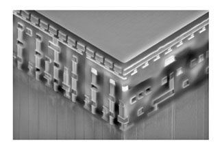
Figure 2: RRAMs simplicity, stackability, and CMOS compatibility reduce costs.
RRAM technology can be based on three simple layers: a nonmetallic bottom electrode, an amorphous silicon switching medium, and a metallic top electrode. The resistance switching mechanism is based on the formation of a filament in the switching material when a voltage is applied between the two electrodes. The RAM can be manufactured at the back-end-of-line of any standard CMOS foundry with very limited additional costs.
An example RRAM
Crossbar’s RRAM technology has been highlighted as a potential candidate for next-generation storage technology. We have successfully developed a demonstration product in a commercial fab by manufacturing a fully integrated monolithic CMOS controller and RRAM array.
The steps we are taking right now lead toward mainstream adoption, including bringing our existing technology to a fab and migrating it to 55- and 40-nm nodes, which we are doing right now. Once that’s completed we will start the embedded licensing business, as well as the standalone code and data business. In the next nine months we’ll be ready for a qualification cycle and for accessing customer requirements.
Advertisement
Learn more about Crossbar


