Nanometer-scale ferroelectrics on plastic target energy-harvesting arrays
Using a technique known as thermochemical nanolithography (TCNL), researchers Georgia Institute of Technology can fabricate nanometer-scale ferroelectric structures directly on flexible plastic substrates that would be unable to withstand the processing temperatures normally required to create such nanostructures.
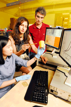
Postdoctoral fellow Suenne Kim holds a sample of flexible polyimide substrate used to produce ferroelectric nanostructures. Assistant professor Nazanin Bassiri-Gharb points to a feature on the material, while graduate research assistant Yaser Bastani observes.
The technique uses a heated atomic force microscope (AFM) tip to produce patterns and could facilitate high-density, low-cost production of complex ferroelectric structures for energy harvesting arrays, sensors and actuators in nano-electromechanical systems (NEMS) and micro-electromechanical systems (MEMS). The research was sponsored by the National Science Foundation and the U.S. Department of Energy. In addition to the Georgia Tech researchers, the work also involved scientists from the University of Illinois Urbana-Champaign and the University of Nebraska Lincoln.
Researchers say they can directly create piezoelectric materials on flexible substrates for use in energy harvesting and other applications. The structures are directly grown with a CMOS-compatible process and are patterned at very small scales. The scientists produced wires approximately 30 nm wide and spheres with diameters of approximately 10 nm using the patterning technique. Spheres targeting ferroelectric memory were fabricated at densities exceeding 200 Gbytes/in.2
The ferroelectric materials exhibit charge-generating piezoelectric responses an order of magnitude larger than those from materials such as aluminum nitride or zinc oxide. The polarization of the materials can be easily and rapidly changed, giving them potential application as random access memory elements. But the materials can be difficult to fabricate, requiring temperatures greater than 600C for crystallization. Chemical etching techniques produce grain sizes as large as the nanoscale features researchers would like to produce, while physical etching processes damage the structures and reduce their attractive properties. Until now, these challenges required that ferroelectric structures be grown on a single-crystal substrate compatible with high temperatures and then transferred to a flexible substrate for use in energy-harvesting.
The thermochemical nanolithography process uses extremely localized heating on the AFM tip to form structures only where the resistively-heated AFM tip contacts a precursor material. A computer controls the AFM writing, allowing the researchers to create patterns of crystallized material where desired. To create energy-harvesting structures, for example, lines corresponding to ferroelectric nanowires can be drawn along the direction in which strain would be applied.
To begin the fabrication, a sol-gel precursor material is applied to a substrate with a standard spin-coating method, then briefly heated to approximately 250C to drive off the organic solvents. The researchers have used polyimide, glass and silicon substrates, but in principle, any material able to withstand the 250C heating step could be used. Structures have been made from Pb(ZrTi)O3—known as PZT, and PbTiO3—known as PTO.
As a next step, the researchers plan to use arrays of AFM tips to produce larger patterned areas, and improve the heated AFM tips to operate for longer periods of time. Ultimately, arrays of AFM tips under computer control could produce complete devices, providing an alternative to current fabrication techniques. Find more information at http://www.gatech.edu/newsroom/release.html?nid=68848
Paul O’Shea
Advertisement
Learn more about Electronic Products Magazine


