As high-speed data technologies evolve to become faster and smaller, sensitivity to electrostatic discharge (ESD) and lightning surges has increased. Now more than ever, a robust and effective surge protection solution is needed that prevents damage, but does not hamper the high-frequency operation of the system. The new transient-current suppressor (TCS) technology offers a brand new approach to meet these demanding requirements.
Some estimates for the actual cost of ESD damage to the electronics industry run into the billions of dollars. According to the Insurance Information Institute, damages caused by lightning on average have increased in the United States by 5.5% over last year, driven primarily by a rise in the number and value of consumer electronics. Lightning strikes cost insurers an average of $5,112 a claim in 2011, compared with $4,846 the previous year. Due to these high costs and potential damage to electronic equipment, it’s more important than ever to have adequate circuit protection for high-speed data applications.
This article reviews conventional single-stage protection using a voltage-limiting device such as a transient-voltage suppressor (TVS) diode and highlights the limitations of this protection method. A new approach to circuit protection will be presented that introduces new TCS technology. This new approach uses TCS devices in series with the protected signal line, in a two-stage configuration together with a voltage-limiting device. The performance and protection efficiency advantages of this new two-stage protection device turns out to be far superior to that of conventional TVS technologies.
Single-stage circuit protection
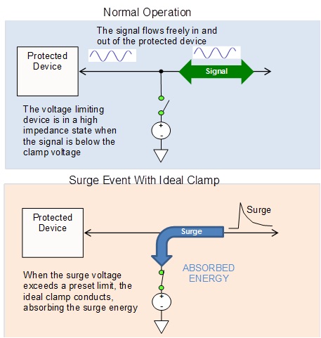
TVS diodes are electronic protection devices that absorb ESD energy at the interface of a design. The basic operation of a TVS diode is shown in Fig. 1 .
A TVS diode typically appears as high impedance in the normal range of the signal working voltage that passes over the line. When a surge at the interface exceeds a preset limit, the TVS diode becomes conductive, quickly limiting the voltage from rising above this safe level. The ideal TVS diode creates a “brick wall” clamping electrical characteristic that causes no interference to the normal signal, yet prevents the voltage at the interface from reaching an unsafe level.

Fig. 1: Basic operation of an ideal voltage-limiting device.
In reality, the characteristics of semiconductor TVS diodes differ from that of the vertical characteristic of the ideal clamping device. Although the real TVS diode exhibits high resistance at lower voltages, as the voltage increases a finite “leakage” current begins to flow near the breakdown voltage of the junction. This results in an actual clamping characteristic that is much softer than the abrupt vertical “brick wall” characteristic of the ideal clamp. The larger the TVS device, the more leakage can occur which can negatively impact the operation of the circuit, particularly at higher temperatures. The clamping voltage chosen must be higher than ideal in order to make allowance for this soft transition into clamping behavior. The actual clamp voltage selected for the circuit is a compromise between a high enough level that does not interfere with the signal, and a low enough voltage to maximize protection.
Simply connecting a TVS diode between an interface and ground is not always effective in protecting the low-voltage device driving that interface. For example, with a typical TVS device, the peak voltage across it may reach 20 V during a discharge of 11 A. This is far beyond the absolute maximum ratings of many low-voltage semiconductor technologies. Instead of shielding the interface device from the surge, the TVS diode simply diverts a portion of the energy away, leaving a portion of the surge energy to propagate into the protected circuit. A high level of “let-through” energy, as it is often termed, may result in equipment damage under surge conditions in harsh or exposed environments, where exposure to high-surge energies may be commonplace.
Two-stage circuit protection: A new approach
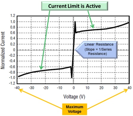
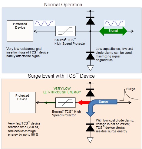
The TCS device is a new circuit protection approach that greatly improves the level of defense when used in series with the protected signal line in a two-stage design together with a voltage-limiting device. The characteristics of the TCS device is shown in Fig. 2 . When normal signal current is low, the TCS device behaves just like a low-value resistor. Under surge conditions and when the current is driven above a safe level, the TCS device transitions very quickly into a current-limiting state. Figure 3 shows the TCS device configuration and circuit symbol.

Fig. 2: Actual I-V curve of a TCS device.

Fig. 3: Implementation of a TCS device in a circuit protection solution.
The TCS device adds a current-limiting stage in series with the protected device to complement the characteristics of the voltage-limiting device, which helps to reduce stress. The voltage at the interface increases when a surge occurs, causing current to flow through the TCS device. As the current limit is reached, the TCS device prevents further increase in current, allowing the voltage across itself to increase. This presents a very high blocking resistance, as current is limited to a near-constant level. As the current is limited, the voltage at the protected device no longer rises, and it is kept at a safe level. On the other side of the TCS device, the voltage continues to rise until the activation voltage of the voltage clamping device is reached. Both the onset of the clamping, and the maximum voltage clamp voltage can be much higher than a TVS by itself, as the TCS device blocks this voltage. The peak clamping voltage may rise as high as the ±40-V maximum voltage rating of the TCS device, allowing the use of simple low-cost, low-capacitance diode rail clamps for most application. The overall performance of the protection stage, as experienced by the driver, very closely resembles the operation of the ideal “brick wall” clamp.
As its name suggests, the TCS device is directly analogous to the TVS diode. The TVS diode limits transient voltages, and the TCS device limits transient currents. The characteristics of the TCS device, like the punch-through TVS diode, also exhibit a degree of foldback, which causes the current to drop approximately 30% from its maximum value as the voltage increases further. This foldback further improves transient power handling in the TCS device and minimizes stress in the protected device.
The normal response time to achieve limiting operation is less than 50 ns. The speed of the current-limiting operation of the TCS device is ideal for protecting against all standard lightning surge test waveforms (1.2/50 μs, 10/1,000 μs, etc.), including high-frequency avionics requirements.
New TCS devices provide an effective ESD and surge protection solution. In contrast to conventional TVS diodes, enhanced protection and functionality is not at the expense of adding capacitive devices that decrease bandwidth and reduce data rate performance. Using a two-stage protection design that combines the current limiting properties of a TCS device with the voltage-limiting properties of a TVS diode or clamp diodes offers a more-robust, low-cost circuit protection solution without compromising circuit performance.
Advertisement
Learn more about Bourns


