It’s no secret that the mantra in chip design today is “use less power.” The advent of the Internet of Things (IoT) brings in a new corollary: “Use less average power” by operating at ultra-low power in standby yet be ready to come alive immediately. Current memory technologies make achieving both attributes simultaneously difficult, but Renesas Electronics Corporation has responded to the challenge with new embedded SRAM technology.
Any battery-operated design needs to use as little power as possible. Low-powered operation is especially important in the IoT, more so than a smartphone, because many points on the IoT are physically remote, and changing or recharging batteries would be a major hassle, if not dangerous or even impossible. For this reason, many IoT nodes are designed to spend most of their time asleep and wake up only occasionally in reaction to a local stimulus, or to make a report as requested by another point on the network. Then they must get up and run as fast as possible to finish their task quickly and go back to sleep, minimizing their average energy usage.
Unfortunately, holding data in SRAM during this sleep mode takes way too much power. Designers currently respond to this issue by simply offloading SRAM contents to nonvolatile memory and then shutting off power to the SRAM during sleep. The problem is that, for some IoT duty cycles, this method can be ineffective, and some instances can even cause actual increases in power consumption.
Renesas seems to have found an answer to this problem. The key to reducing SRAM on/sleep power ratio has been to reduce transistor leakage current, which Renesas has done by deploying its 65-nm silicon-on-thin-buried oxide (SOTB) process to the development of embedded SRAM. Renesas’ SOTB process utilizes a dopant-less channel structure, made possible through its buried oxide layer. The result is far less variation in transistor threshold characteristics which, in turn, makes it possible for transistors to perform well at voltages as low as 0.5 V.
An on-chip regulator controls substrate bias, which determines if the device operates in an operating mode or in the standby mode. Setting the substrate potential to forward bias allows for a rapid read access time. Standby mode is achieved by applying a reverse bias to the substrate, which reduces leakage current dramatically.
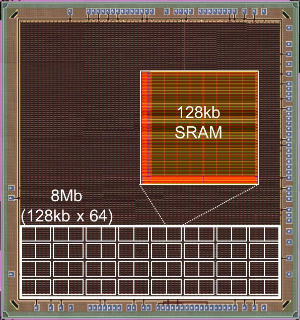
Aimed at developers of application-specific standard products (ASSP), the technology is not available as an off-the-shelf SRAM device. But Renesas has created a prototype SRAM to demonstrate the technology. This prototype has achieved a readout time of 1.8 ns when it is “live” and yet only requires 13.7 nW/Mbit in standby. This is only one-thousandth of the memory’s power consumption during its normal mode.

Renesas Embedded SRAM. Source: Renesas.
Renesas expects that its new process will contribute towards development of IoT nodes that need no maintenance or battery replacements while offering long life. By allowing rapid startup, high-speed operation while live, and substantially reduced leakage current in sleep mode, SRAMs based on the Renesas SOBT technology can help IoT designs operate at miniscule average power levels.
Advertisement
Learn more about Electronic Products Magazine


